
February 5, 2024
Shop NowIn the intricate realm of semiconductor production, where minuscule components orchestrate the symphony of technological advancement, the role of wafer testing and quality control is paramount. The journey from raw materials to a finished semiconductor device is fraught with challenges, making the rigorous evaluation of wafers critical. This blog discusses the methods and technological advances used in wafer testing, offering insights into the careful processes that maintain the highest levels of quality control.
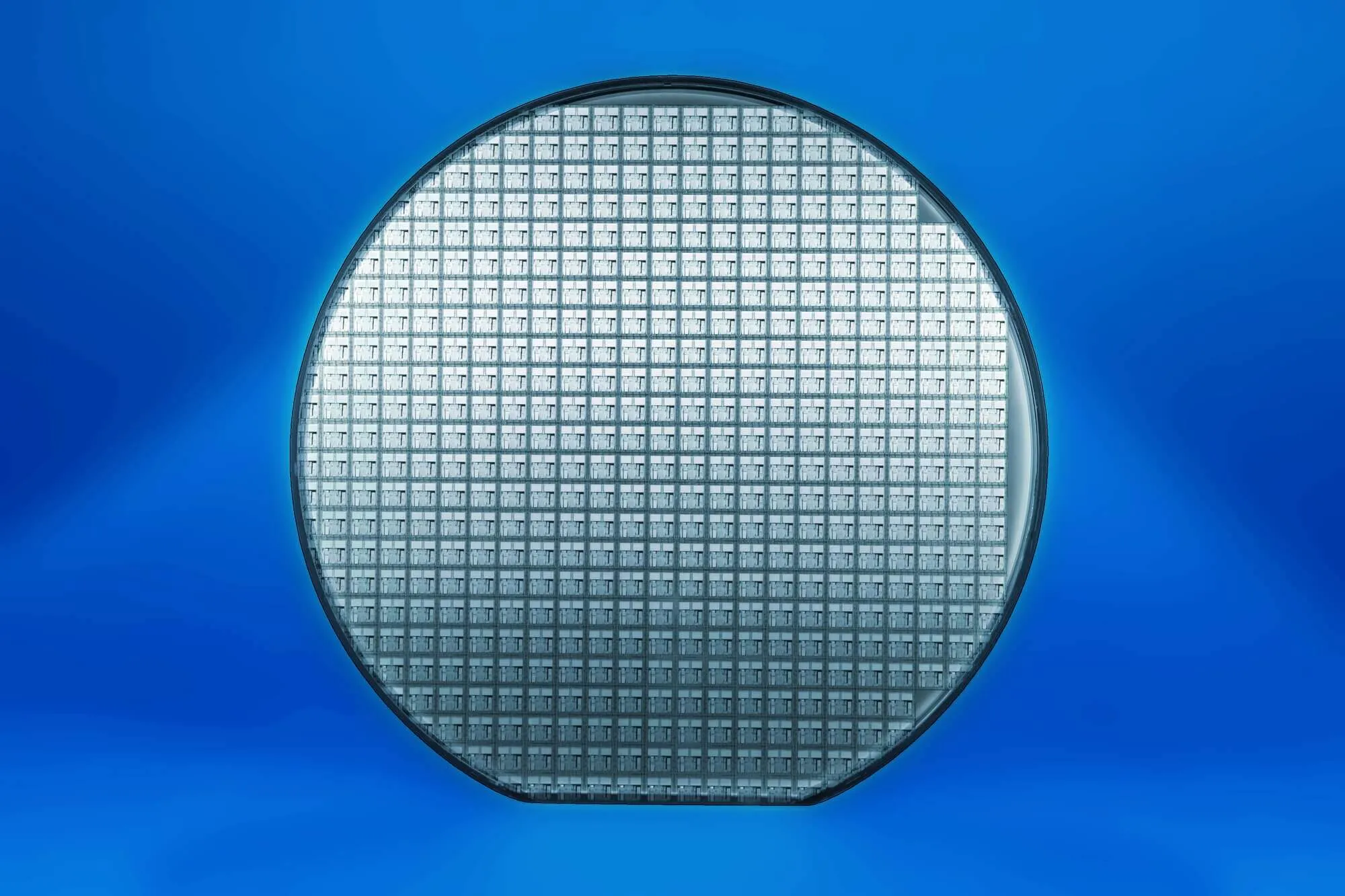
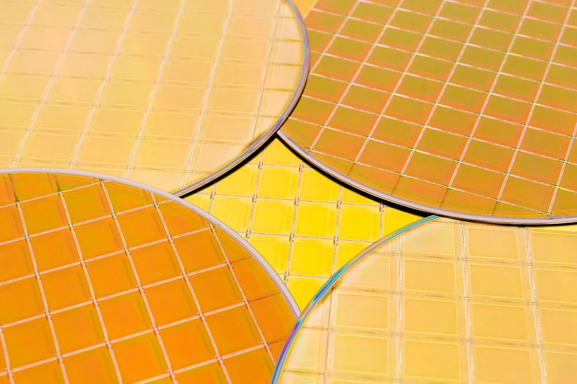
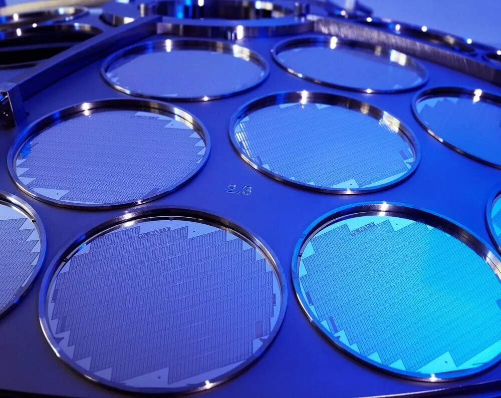
Semiconductor wafers serve as the canvas upon which the intricate patterns of electronic circuits are etched. Before these wafers become the core of our electronic products, they undergo a series of tests to validate their functionality, reliability, and conformity to specific requirements.
At the forefront of wafer testing methodologies is electrical testing. This involves probing the wafer for electrical characteristics, ensuring that each component functions as intended. Key parameters such as voltage, current, and resistance are measured to identify defects or inconsistencies. Automated test equipment (ATE) plays a pivotal role in this process, efficiently conducting high-throughput testing across multiple wafers.
Probe testing, or wafer probing, is a method where a set of probes make contact with specific points on the wafer's surface to assess its electrical performance. This method is particularly useful for identifying defects in individual components before the entire wafer is processed further.
The visual inspection of wafers is another crucial aspect of quality control. Optical inspection techniques utilize advanced imaging systems to identify surface defects, contamination, or irregularities in the patterns etched onto the wafer. High-resolution microscopy and machine vision technologies are employed to scrutinize the wafer surface with precision.
X-ray and acoustic microscopy techniques offer non-destructive insights into the internal structure of the wafer. X-ray imaging can reveal hidden defects or inconsistencies within the layers of the semiconductor, while acoustic microscopy uses sound waves to identify variations in material density, aiding in the detection of defects that may impact performance.
The precise dimensions of features on a wafer are critical for ensuring the functionality and reliability of semiconductor devices. Metrology techniques, such as scanning electron microscopy (SEM) and atomic force microscopy (AFM), are employed for dimensional analysis, helping to maintain the accuracy of the manufacturing process.
DR-SEM is a specialized technique for inspecting and analyzing defects on a wafer surface at high magnification. This method assists in identifying the root causes of defects, enabling manufacturers to implement corrective measures and enhance the overall yield of the manufacturing process.
Wafer-level reliability testing is conducted to simulate the operational conditions that a semiconductor device might encounter during its lifespan. This includes exposure to temperature extremes, voltage stress, and other environmental factors. WLRT helps assess the long-term reliability and durability of the semiconductor, ensuring it meets stringent quality standards.
Machine learning and artificial intelligence are increasingly integrated into wafer testing processes for automated defect classification. These technologies enable the identification and categorization of defects with remarkable speed and accuracy, enhancing the efficiency of quality control procedures.
Implementing statistical process control methodologies allows manufacturers to monitor and control the wafer fabrication process in real-time. By analyzing data from various stages of production, SPC helps identify trends, patterns, or anomalies that may impact the quality of the final product.
Thermal testing is indispensable in assessing the thermal performance of semiconductor wafers. Excessive heat can degrade the functionality and lifespan of electronic components. Thermal imaging and testing methodologies help identify potential hotspots or thermal irregularities across the wafer, ensuring optimal heat dissipation and preventing overheating issues in the final product.
Particle contamination on the wafer's surface can lead to defects and compromises in device performance. Stringent cleanliness standards are maintained through advanced particle detection and control methods. Cleanroom environments, air filtration systems, and particle monitoring technologies contribute to minimizing particle contamination during wafer manufacturing.
CMP is crucial in wafer manufacturing, smoothing, and leveling the wafer surface. Monitoring CMP procedures promotes uniform material removal and eliminates uneven surfaces, which can lead to faults. Real-time monitoring of CMP parameters, such as pressure and slurry composition, enhances the precision of the planarization process.
Electromigration is a phenomenon where metal atoms migrate within a conductor due to the passage of electric current, potentially causing reliability issues. Electromigration testing involves subjecting the wafer to prolonged periods of current flow to assess the resistance to this phenomenon. This helps in identifying potential weak points and enhancing the reliability of interconnects.
Simulating real-world environmental conditions is crucial to ensuring the reliability of semiconductor devices. Environmental stress testing involves subjecting wafers to extremes of temperature, humidity, and other environmental factors. By replicating harsh conditions, manufacturers can identify vulnerabilities and make design improvements to enhance overall device durability.
Wafer-level packaging involves encapsulating the wafer with multiple layers to protect the semiconductor components. Inspection techniques for wafer-level packaging include X-ray inspection, thermal imaging, and visual inspections to verify the integrity of the packaging process, ensuring that the final product meets quality standards.
When defects are identified, failure analysis becomes crucial in determining the root cause. Techniques such as focused ion beam (FIB) microscopy and transmission electron microscopy (TEM) enable in-depth analysis of defects at the nanoscale, aiding in the identification of issues and informing process improvements.
Implementing real-time in-process monitoring and control systems allows manufacturers to identify deviations from the desired specifications during various stages of wafer manufacturing. This proactive approach enables rapid adjustments, minimizing the impact of potential defects on the final product.
Marking wafers with unique identifiers and implementing traceability systems enhance quality control by allowing manufacturers to track each wafer throughout the production process. This retains responsibility and helps to identify any abnormalities or departures from quality standards.
The incorporation of smart sensors within manufacturing equipment enables continuous monitoring of key parameters. These sensors provide real-time data, contributing to predictive maintenance strategies and allowing for immediate corrective actions when deviations are detected.
The testing of wafers and quality control measures in semiconductor production is pivotal in ensuring the reliability and functionality of the electronic devices we rely on daily. From electrical testing to advanced imaging techniques, the methodologies woven into wafer testing serve as a cornerstone for the semiconductor industry, advancing innovation and pushing the boundaries of technological possibilities.
As we go through the ever-evolving landscape of semiconductor manufacturing, the commitment to precision and quality control remains unwavering, shaping the future of electronic advancements. Call us to order!


