Float-zone (FZ) wafers have emerged as a highly desirable material in the semiconductor industry due to their unique properties, such as high purity and low defect density. These attributes make them well-suited for high-power electronic devices requiring superior performance, efficiency, and reliability. This article explores the advantages of FZ wafers in high-power electronic applications and examines the challenges and opportunities associated with their use.
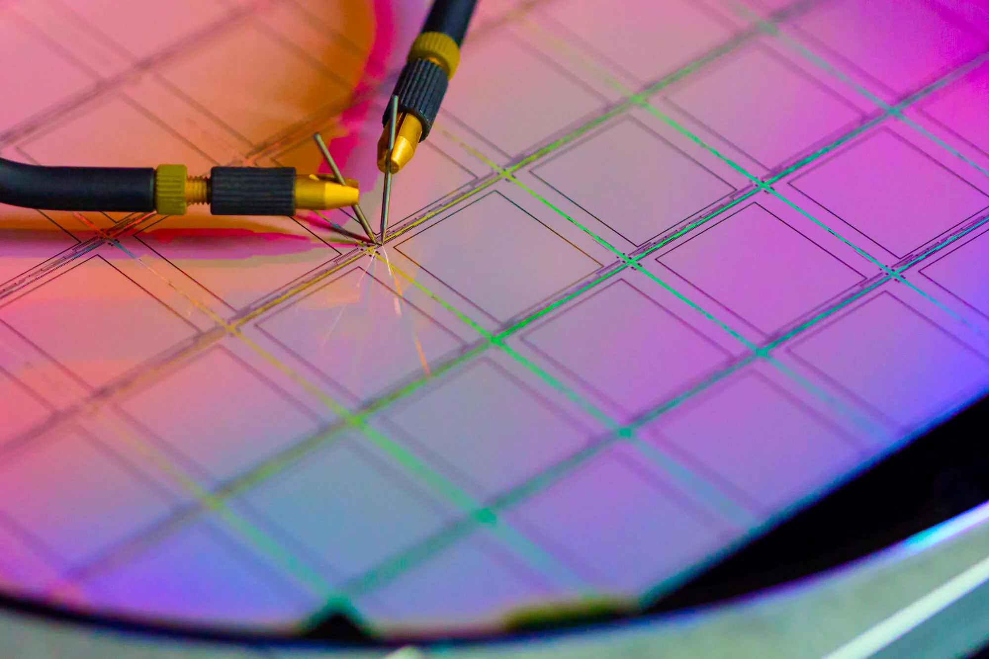
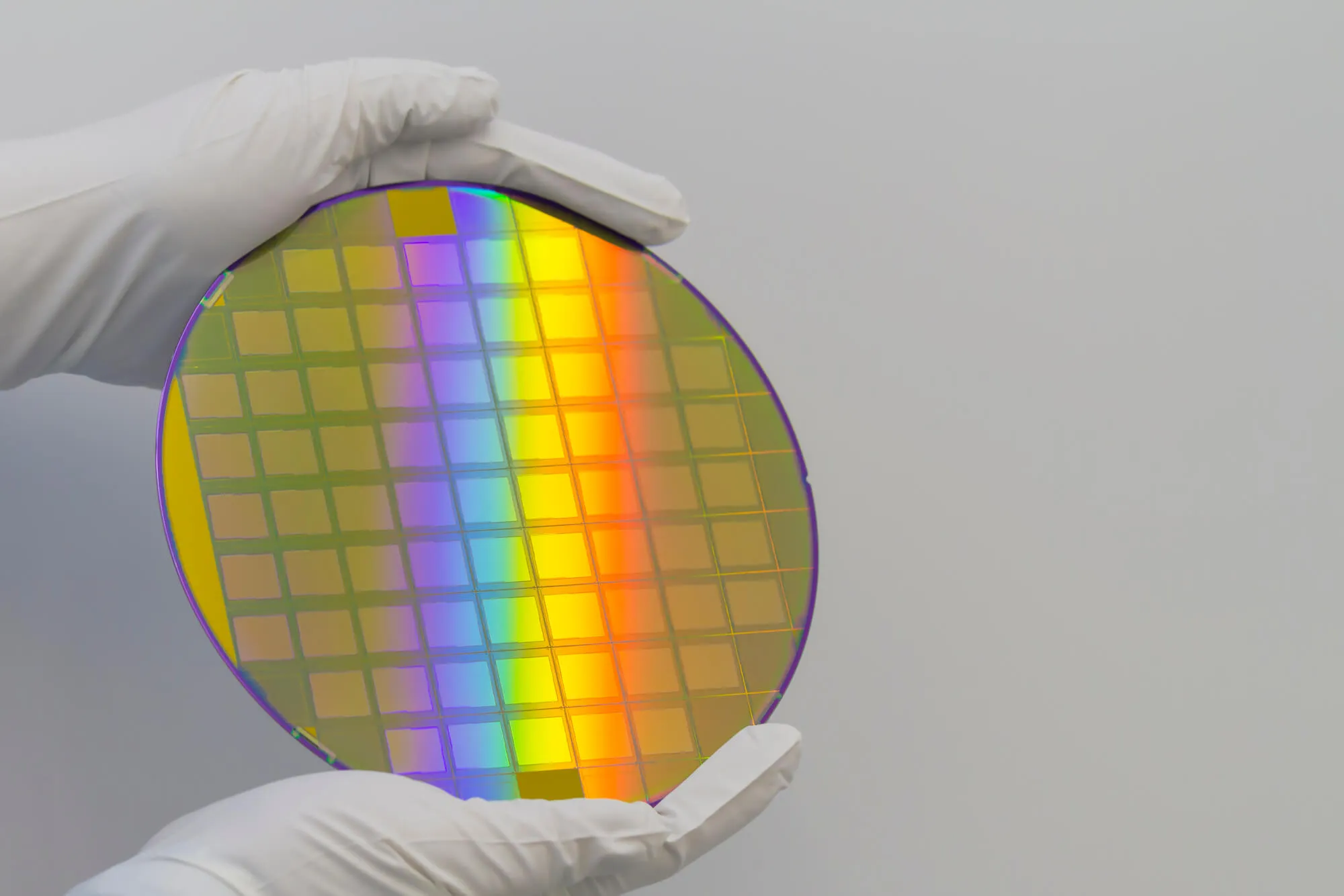
FZ wafers, or float-zone wafers, are high-purity semiconductor materials that manufacture electronic and optoelectronic devices. The float-zone process, also known as the zone-melting process, is a crystal growth technique that involves the slow melting and recrystallization of a silicon rod in a controlled environment. This method produces wafers with low impurities and defects, making them ideal for certain applications.
Some common uses of FZ wafers include:
FZ wafers are high-purity semiconductor materials used in various electronic and optoelectronic applications, particularly where device performance, efficiency, and reliability are crucial. Their unique properties make them attractive for high-power electronics, photovoltaics, optoelectronics, high-frequency devices, and radiation-hardened electronics.
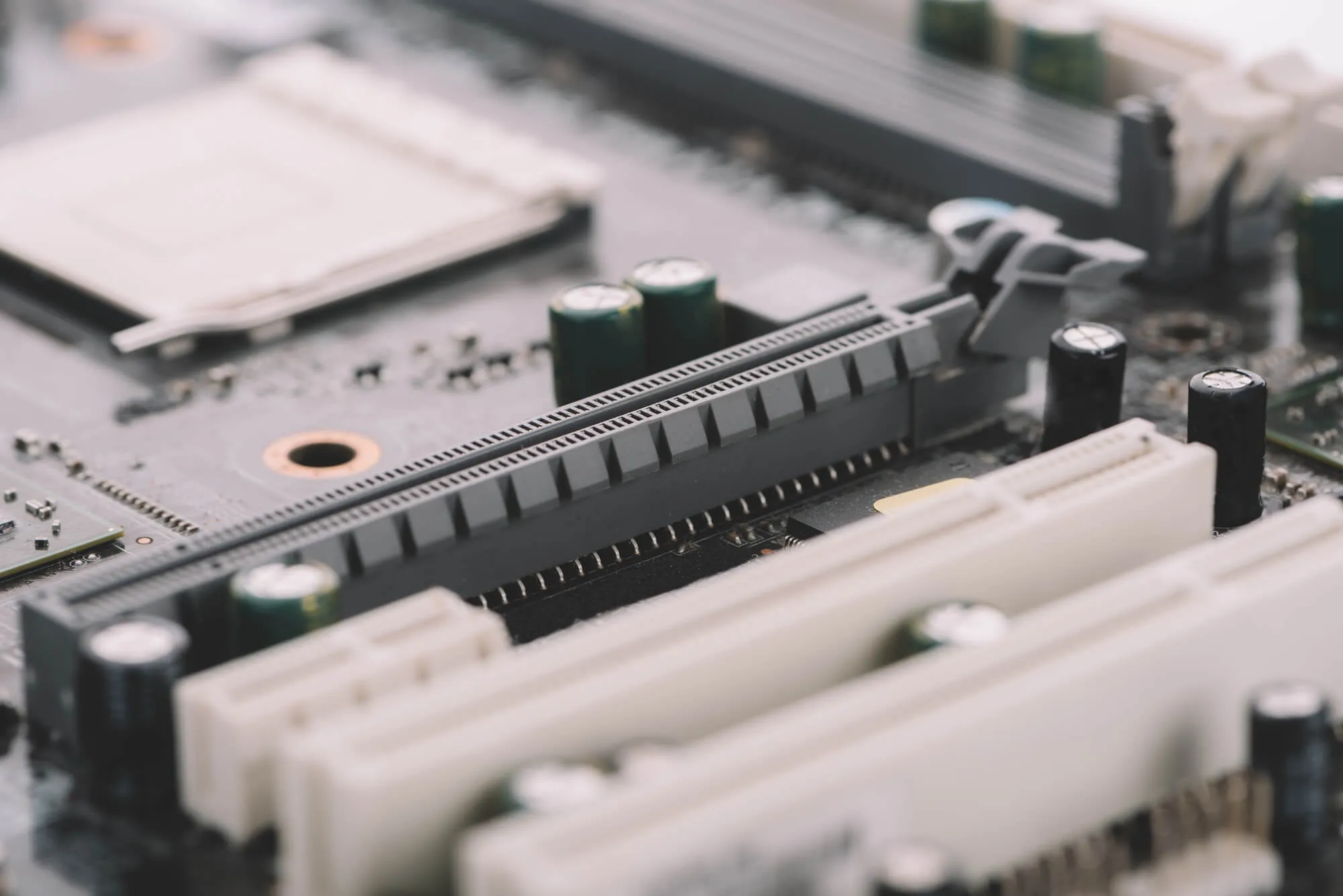
High-power electronic devices are components designed to handle and control large amounts of electrical power. These devices typically operate at high voltage and current levels, requiring them to exhibit high efficiency, reliability, and thermal stability. High-power electronic devices are critical in various applications, such as power conversion, motor drives, power transmission, and renewable energy systems.
Power transistors are essential components in various electronic systems that amplify and switch electrical signals. Common types of power transistors include metal-oxide-semiconductor field-effect transistors (MOSFETs), insulated-gate bipolar transistors (IGBTs), and silicon carbide (SiC)-based devices. They are crucial in power conversion, motor drives, and renewable energy systems, where high efficiency and reliability are vital.
Power diodes are semiconductor devices that allow current flow in one direction while blocking it in the opposite direction. Key types of power diodes include Schottky diodes and PIN diodes. They are commonly used in rectifiers, voltage regulators, and power supplies, ensuring stable and efficient operation in various electronic systems.
Other high-power electronic components, such as thyristors, gate turn-off thyristors (GTOs), and integrated emitter turn-off thyristors (IEGTs), also play critical roles in high-voltage power transmission and industrial equipment. These components help manage and control electrical energy in demanding environments where performance and durability are paramount.
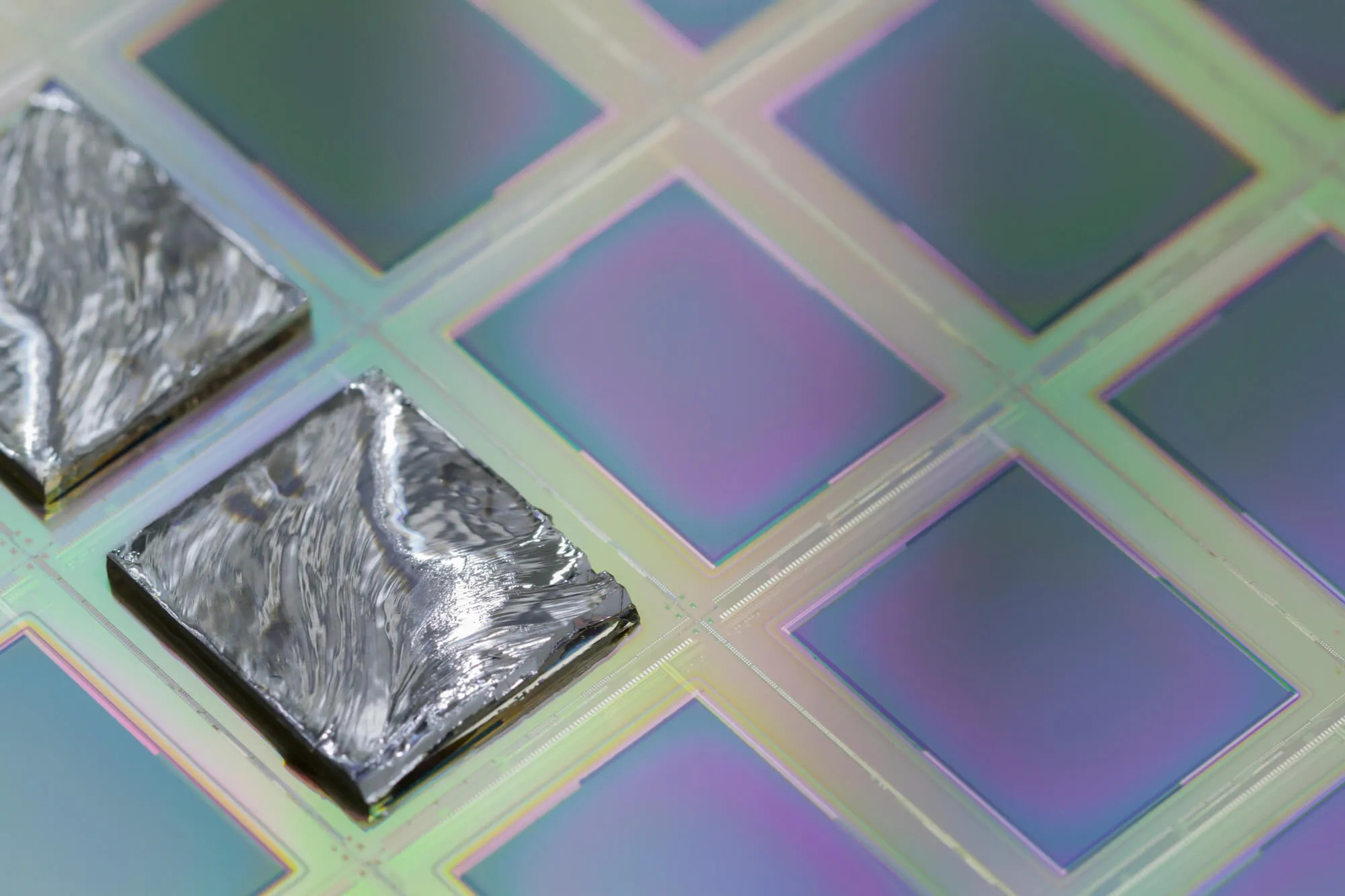
FZ wafers offer superior material purity to Czochralski (CZ) wafers due to their unique manufacturing process, which minimizes impurities and crystal defects. This enhanced purity improves device performance and reliability, making FZ wafers an attractive option for high-power electronics.
The high carrier mobility and breakdown voltage of FZ wafers contribute to reduced power losses and increased energy efficiency in high-power electronic devices. These properties enable the development of advanced components that can perform optimally under high voltage and current conditions.
FZ wafers exhibit high thermal conductivity and resistance to thermal stress, allowing devices to maintain performance even at elevated temperatures. This is particularly important in high-power electronics, where temperature management ensures long-term reliability and prevents premature device failure.
Despite their advantages, FZ wafers face several material and process limitations in manufacturing. Device fabrication and integration with other semiconductor materials also present challenges that must be overcome to exploit the potential of FZ wafers in high-power electronics fully.
The demand for high-power electronic devices across various industries continues to grow, driving interest in FZ wafers. However, alternative semiconductor materials, such as SiC and gallium nitride (GaN), also compete for market share, making it essential for FZ wafers to demonstrate distinct advantages to maintain a competitive edge.
Ongoing research and development efforts aim to improve FZ wafer manufacturing techniques and explore new high-power electronic device designs and materials. Innovations in these areas have the potential to overcome existing challenges and expand the applications of FZ wafers in high-power electronics, further solidifying their importance in the industry.
The Potential of FZ Wafers
Their unique properties, such as high material purity, enhanced electrical properties, and thermal stability, make them well-suited for applications in power conversion, motor drives, renewable energy systems, and more. However, to fully realize the potential of FZ wafers in high-power electronics, technical challenges related to manufacturing, device fabrication, and integration with other semiconductor materials must be addressed.
Ongoing research and development efforts play a crucial role in overcoming these challenges and expanding the applications of FZ wafers in the high-power electronics market. The impact of FZ wafers on the performance, efficiency, and reliability of high-power electronics is undeniable. As research continues to advance, FZ wafers are poised to play an increasingly significant role in shaping the future of the high-power electronics industry, driving innovation, and enabling a new generation of advanced devices and applications.
At Wafer World, we provide our clients with high-quality wafers and silicon wafers to help them create new or existing technologies. If you're interested in learning more about our products, give us a call today!


