Laser marking is the process of subjecting bare silicon wafers to laser radiation to inscribe specific markings on their surfaces.

Marking silicon wafers provides fabricators with essential product identification. Wafers are produced in batches that comprise hundreds of substrates. Manufacturers must institute a means to trace which wafer went to which client. If there’s a quality control issue, customers only need to look at the lot and batch numbers marked on the wafer’s surface.
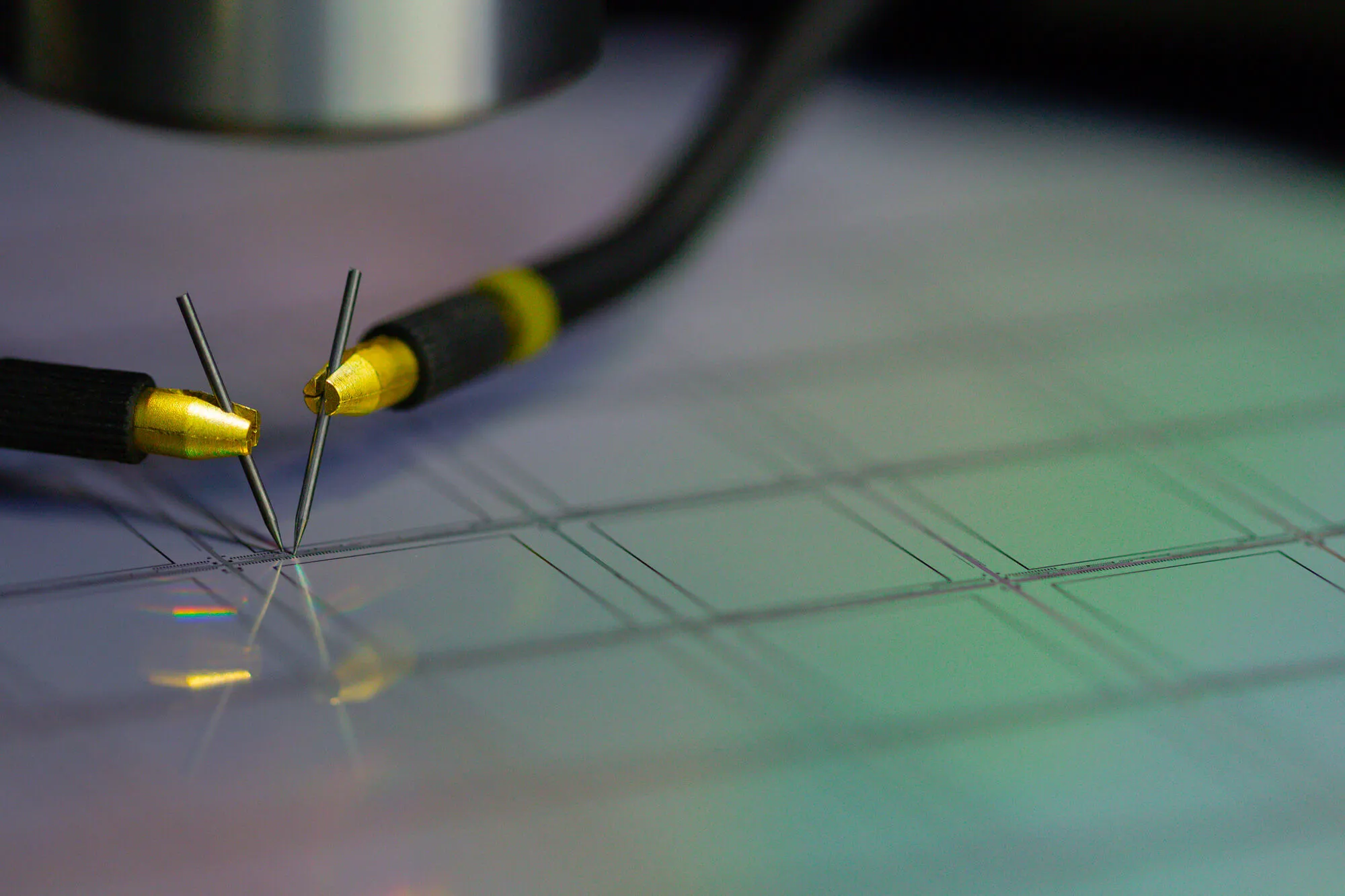
The process involves using a focused laser beam to scribe markings below a wafer’s surface. A computer guides the laser emitter using a digital template. Laser markers fire low-powered beams in controlled pulses to minimize penetration.
A laser diode emits radiation, which is one of the common causes of damage to wafers. The marking system must be precise and accurate to avoid injury to the semiconductor. Fortunately, laser marking machines are accurate even in the micrometer thresholds.
Marking with a laser is a relatively quick process that requires no human intervention except when loading the wafers into the machine and previewing the design on a screen. All the operator needs to do is push a button to initiate the process.
A robotic arm will take the wafer and align it with the marking emitter, exposing the semiconductor to laser radiation. The arm will extract the semiconductor and transfer it to a receiving box.
The machine’s precision allows it to heat the wafer at a point below the surface without penetrating through the material. The device can be set to make marks up to 100 micrometers deep into the semiconductor. The resulting pattern is also permanent and non-fading.
Laser marking devices don’t consume excessive energy since they don’t need to penetrate the wafer’s surface. These machines require about 50-kilowatt hours of power per month. This makes the gadget an energy-saving device that helps minimize the production facility’s carbon footprint.
.jpg)
We take care not to subject our wafers to radiation damage during the marking process. If you’d like a free quote, go ahead and contact us.


