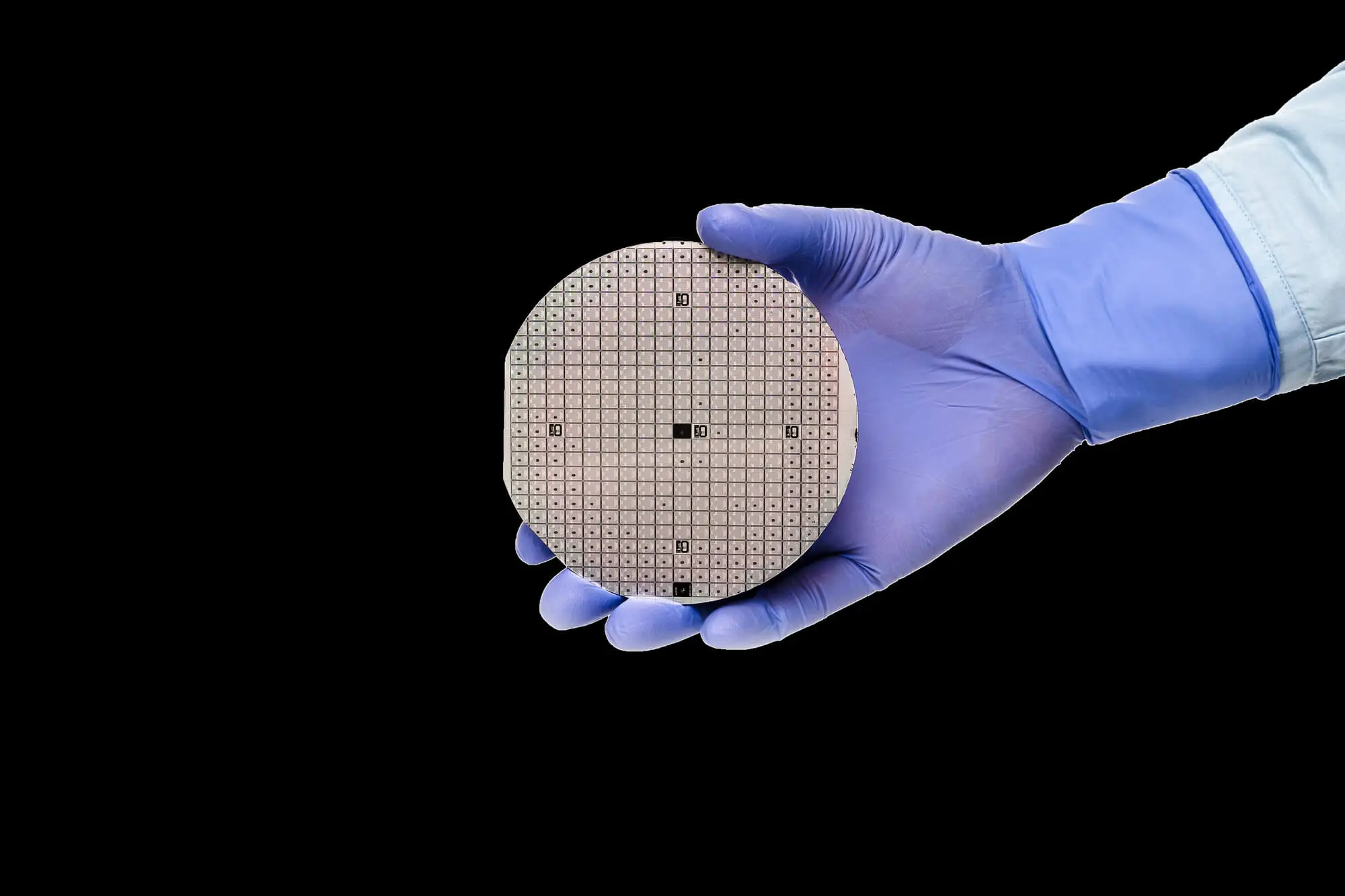
If you want to buy silicon wafers for advanced devices, you've likely encountered SOI wafers. Silicon-On-Insulator (SOI) technology is more than just a niche alternative to bulk silicon; it is a deliberate design choice for applications where performance, isolation, or power efficiency are critical.
An SOI wafer is a layered silicon substrate consisting of three major components:
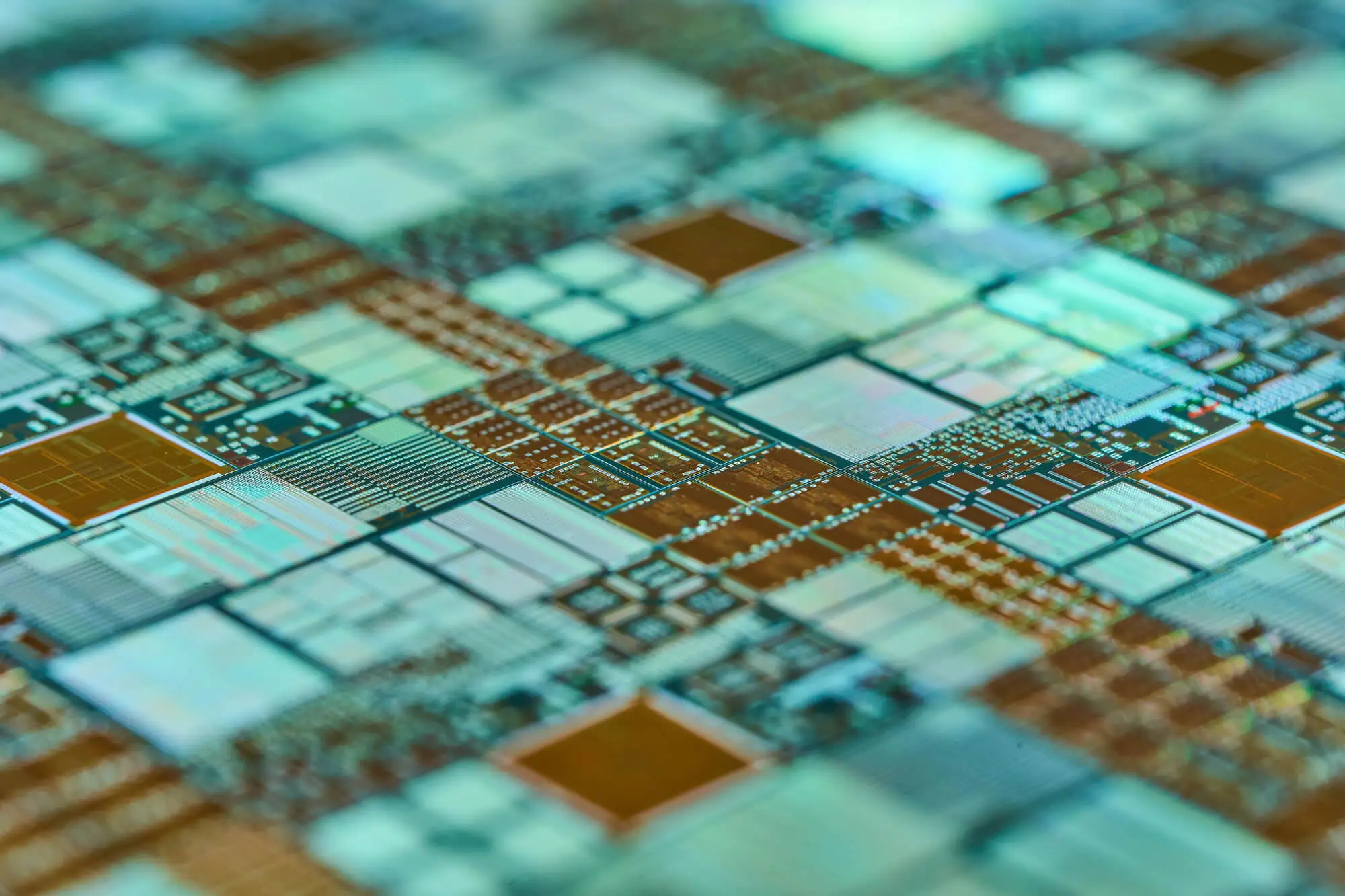
The structure electrically isolates devices from the bulk substrate, significantly reducing parasitic effects that limit performance in standard wafers.
SOI wafers are commonly used in:

SOI wafers aren’t “better” for every application, but they can offer key benefits for specific applications. SOI substrates offer superior electrical isolation, reducing leakage and crosstalk. You should consider SOI wafers if electrical isolation is critical to performance and power efficiency is a design constraint.
However, if none of these apply, standard or epitaxial silicon may be more cost-effective. If you’re still unsure about what’s best for your project, Wafer World can help. Reach out and let us help you find the ideal substrate for your goals!


