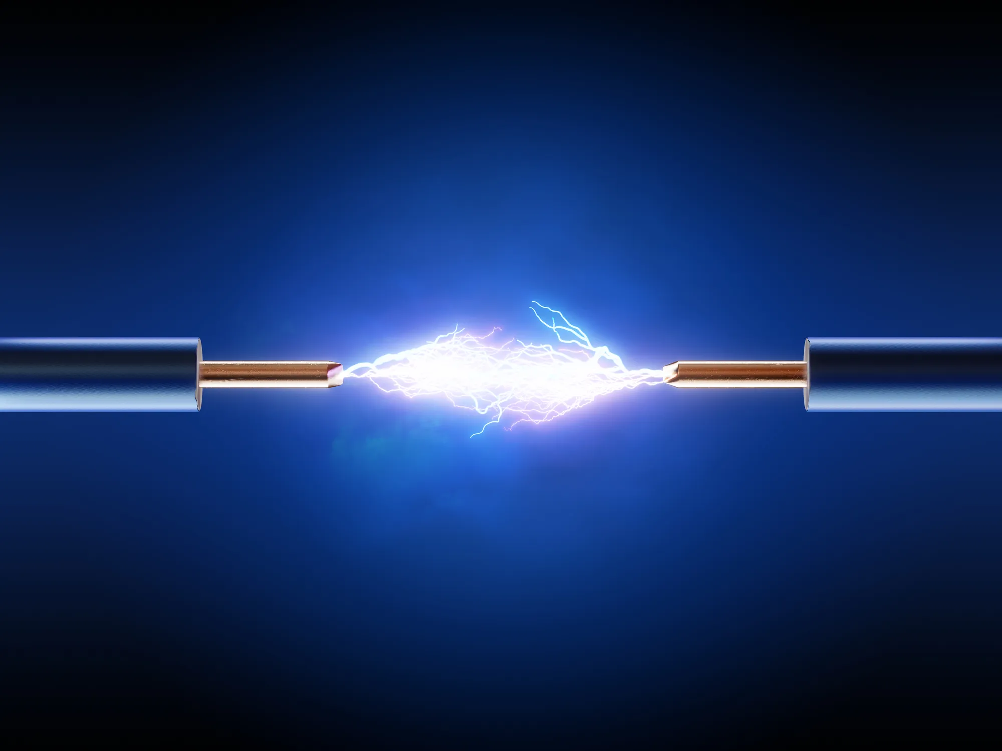
Chips are made up of transistors built on top of a substrate like silicon or an InP wafer. The chip’s functioning depends on how these transistors move or manipulate electrical current. Let’s look at how electrons, the charge carriers, move between these devices.

Benjamin Franklin was one of the first to understand how to manipulate electricity in the 18th century. He described electricity as having positive and negative regions. Franklin’s theory considered the current part with the higher charge positive and the one with the lower charge as negative. The theory posited that the electric current moves from positive to negative.
At that time, scientists have not yet discovered protons and electrons. When they did, it was determined that free electrons are negatively charged and carry more energy than protons. It was also determined that the current moves from negative to positive.
The growth process for wafers is simultaneous with another procedure called doping. Doping adds impure atoms into the semiconductor to make it an insulator or a conductor. This results in two wafer types: the n-type and p-type wafers.
The N-type wafer contains molecules that have more atoms than silicon. Thus, it has free electrons after the rest are bonded with silicon. These free electrons can provide a charge to the circuit when necessary.
On the other hand, the P-type results from bonding silicon with atoms with three outer electrons. A positive “hole” is left when these electrons bond with silicon. This gap will accommodate electrons whenever available.
A transistor switch comprises two N-type wafers with a P-type wafer in between. Gaps called depletion regions are created by this arrangement. Lastly, three electrodes control the current, namely the source, gate, and drain.
The depletion region is a result of interaction between the two wafer types. When placed side by side, the P-side receives the free electrons from the N-type.
The transistor turns itself on and off when it receives voltage from the system. In a computer, tapping the keys or clicking the mouse sends a voltage to specific transistors. The voltage turns the gate positive, allowing the voltage to flow through the source and pull the electrons from the P-type wafer.
This completes the current, which continues to the drain. The switch remains in this state until the voltage is lost. The gate turns negative again at this point, allowing the electrons to return to P-type holes. The depletion region forms again and turns the transistor switch off.
.jpg)
Our wafer products are manufactured with a focus on quality. We strive to maximize production yield for every wafer from our product line. Contact us now for a free quote.


