July 4, 2025
Shop NowGallium Arsenide (GaAs) wafers are widely used to fabricate high-frequency and optoelectronic devices, including RF amplifiers, LEDs, and solar cells. However, due to their high material cost, manufacturers often use GaAs reclaim wafers—that is, previously used substrates that have undergone a “recycling” process to give them a new life.
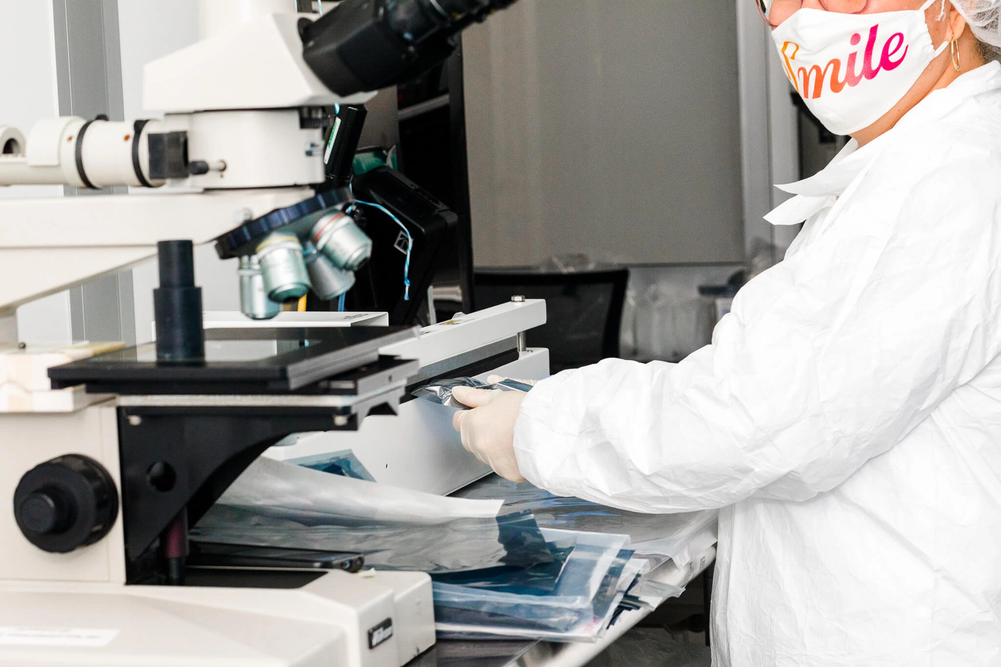
A common concern among buyers is whether the reclaim process results in a loss of quality. To avoid that, reclaimed wafers are put through an extensive quality control process before being put out in the market, and the first step is filtering to determine which wafers can undergo the process.
GaAs reclaim wafers are essentially recycled semiconductor wafers made from gallium arsenide. GaAs is a key material used in high-frequency and high-speed electronic devices, such as microwave and millimeter-wave applications, high-power and high-frequency transistors, and optoelectronic devices.
This is due to this material’s unique electrical and thermal properties. Sadly, gallium arsenide isn’t as widely available as silicon, and manufacturing it can be expensive. So, manufacturers often opt to use reclaimed wafers over brand-new ones to cut down development costs while still enjoying the unique benefits of GaAs.
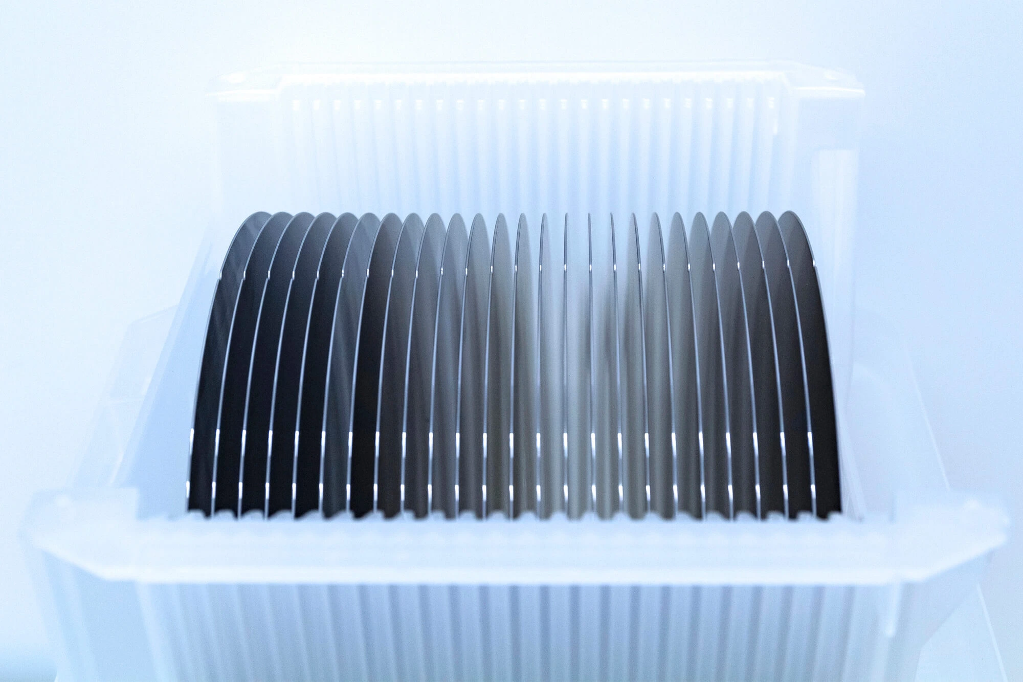
The GaAs reclaim involves refurbishing and reusing wafers already used in semiconductor fabrication processes, including cleaning, surface stripping, and polishing.
However, reclaiming GaAs wafers is not indefinitely sustainable. There comes a point when the reclaim process becomes technically or economically unviable, and here are some pointers that fabs pay attention to before reclaiming a wafer.
Irreversible surface damage is one of the most common reasons a GaAs reclaim wafer becomes non-viable. During device processing and subsequent reclaim cycles, wafers undergo multiple rounds of film deposition, etching, cleaning, and polishing. Over time, these steps can introduce:
If polishing and chemical cleaning can no longer remove these imperfections without compromising wafer thickness or flatness, the wafer is deemed unusable, as surface quality directly impacts device performance.
Each reclaim cycle includes chemical-mechanical polishing (CMP) to restore a smooth, planar surface. However, excessive or uneven polishing can lead to warping, bowing, or non-uniform thickness, particularly in thinner wafers or those with high internal stress.
GaAs is more brittle than silicon, making it more sensitive to mechanical stress and susceptible to cracking.
When wafers deviate beyond flatness or bow specifications—typically on the order of microns—they become incompatible with front-end lithography tools or automated handling systems. At this point, reclaiming further is not practical.
GaAs reclaim wafers typically lose some thickness with every reclaim cycle due to repeated CMP and surface conditioning. Depending on the depth of damage being polished away, the initial wafer thickness may be reduced by 5–10 microns per cycle.
Once the wafer becomes too thin to safely handle, support during processing, or mount on vacuum chucks, it no longer meets the physical criteria for reuse.
For instance, wafers that fall below 500 µm for standard 4-inch GaAs substrates may break more easily during processing or thermal cycling, rendering them unsuitable for further reclaim or reuse.
Edge chipping is frequent in GaAs wafer handling, especially in automated environments. While minor edge damage may be tolerated in early reclaim cycles, progressive edge wear or visible mechanical cracks severely limit wafer integrity and safety.
Cracks increase the risk of wafer breakage and introduce contamination risks to the cleanroom and other wafers. When edge damage exceeds acceptable criteria, the wafer must be discarded for safety and process stability.
As process technology evolves, the specification requirements for reclaimed wafers may become more stringent—especially in high-frequency or optoelectronic R&D. If a reclaimed wafer no longer meets the flatness, cleanliness, or crystallographic orientation required by newer tools or experiments, it becomes functionally obsolete.
Similarly, reclaim wafers used as monitor substrates or for metrology may lose their usefulness if toolsets require different coatings, doping levels, or wafer diameters.
Each reclaim cycle exposes the wafer to thermal, chemical, and mechanical stress. Over time, this can increase dislocation density, create point defects, or even result in microcracks in the crystalline structure.
These defects are particularly detrimental in GaAs because they can significantly degrade electrical and optical performance.
Material characterization can reveal whether or not the crystal quality has degraded beyond usable limits. If so, the wafer can no longer support high-performance device fabrication or testing.
Sometimes, the reclaim process itself becomes economically unjustifiable. As reclaim costs (labor, CMP, cleaning chemicals, inspection) rise or wafer performance degrades, the cost per usable reclaim cycle may exceed the cost of purchasing new test or dummy wafers.
This economic tipping point is often reached after 3–10 reclaim cycles, depending on wafer quality and the intended application.
When deciding whether or not to use reclaim wafers in your project, it’s important to assess each situation individually. GaAs reclaim wafers may no longer be suitable for high-end device fabrication, but they can serve valuable roles in:
Utilizing reclaimed wafers in these tasks can reduce material costs while supporting R&D and manufacturing environments where full-spec wafers are not necessary for functional testing or process refinement.
While GaAs reclaim wafers provide significant cost savings and sustainability benefits, their reuse is ultimately limited by physical, chemical, and economic factors. Excessive surface damage, reduced thickness, loss of flatness, edge defects, or deteriorating crystal quality can all render further reclaiming impractical—or result in sub-par products.
Besides checking the wafer's viability beforehand, GaAs reclaim substrates undergo rigorous quality control measures to ensure they meet industry standards. These processes include cleaning, testing, and refurbishing the wafers to ensure they perform just as well as newly manufactured ones. If you’d like to learn more about the reclaim process at Wafer World, reach out!


