.webp)
As semiconductor wafers acquire more applications throughout all kinds of industries, their levels of specialization in their manufacturing processes also get more complex. Among all, ultra flat wafers are built with the highest specifications, but they also require the most complex handling conditions.
As all industries' demands for ultra thin wafers increased, the need for automated transportation methods that don’t damage the wafer’s integrity also became apparent. Here are some of the current possibilities and challenges in wafer logistics, in an industry where substrates are constantly getting thinner.
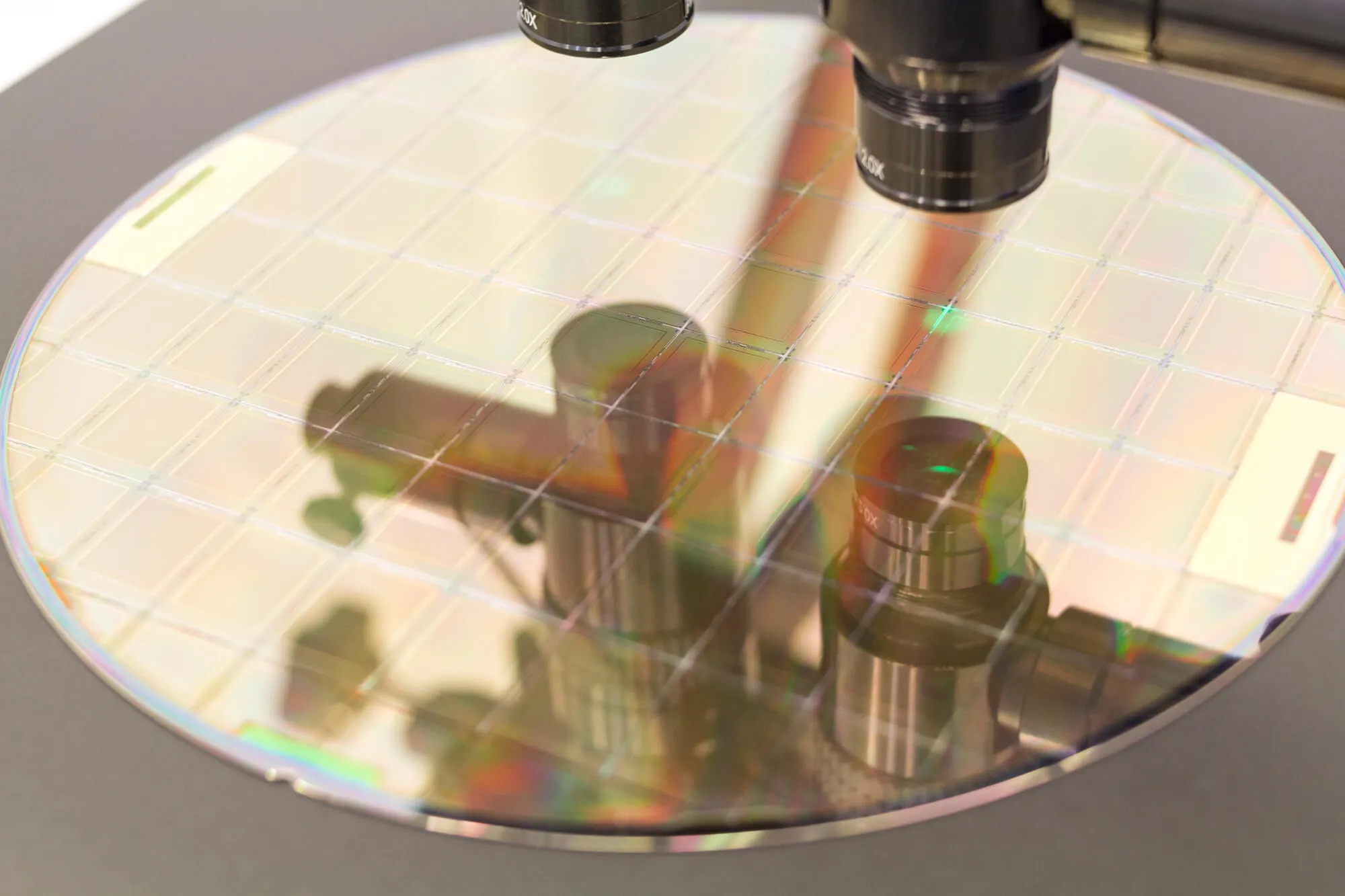
Ultra flat wafers are thin slices of semiconductor material with a thickness generally under 200 μm. A micrometre (μm) or micrometer is a unit of length equaling 1 × 10⁻⁶ metre.
When the term ‘ultra-thin wafers’ emerged, only the mass production of 8-inch wafers of 120 and 70 μm had been achieved. However, today, wafers with thicknesses of 50 μm and 30 μm have also been proven to be viable.
What this demonstrates is how innovative and productive the wafer industry is, with innovation being a constant factor. And as new, and more delicate substrates are developed, industries need to catch up with their machinery and handling methods.
After all, moving these paper-thin discs is no trivial task. But, what makes ultra thin wafers such delicate materials? Here are some facts:
As you can see, due to the characteristics of the material, the handling of thin wafers in-today’s production lines require high standards of quality. Moreover, this has to be done in a way that fulfills the industry’s demand for thin wafers production.
The secret to that lies in automation. With the right technique and the proper tools, handling these delicate materials in mass production can be achieved.

In 2012, the Fraunhofer Institute for Manufacturing Engineering and Automation (IPA) conducted an important experiment on automated handling methods for ultra thin wafers. One of the most successful strategies they found was using Bernoulli Vacuum Grippers to transport wafers.
The Bernoulli Type Gripper is a specialized robotic gripper used to manage delicate objects. It's based on the Bernoulli principle, which describes the inverse relationship between the pressure and velocity of a fluid.
By taking advantage of this phenomenon, Bernoulli Grippers can lift and hold items with minimal contact, making them ideal for handling delicate workpieces like thin cloths, films, and ultra flat wafers.
Here’s the process the investigators described:
The Bernoulli grippers pick up the wafer and lift it vertically. One of the risks to consider at this stage is the possible vibrations caused by the air drag and the inertia force
The wafer is transported to the next step. Further movements in the air can cause vibrations, however, utilizing a vacuum-type gripper helps avoid even stronger damage to the wafer.
During the placement procedure, wafers often need to be blown off. This can cause shifts in the position, which makes repeatable position accuracy in placement difficult. Additionally, observations showed an unsteady way of how the wafer is released from the gripper’s surface.
Pro Tip: The researchers remarked on the need to make an effort to find suitable parameter settings for a reliable pick-&-place application.
Fraunhofer Institute’s study demonstrated that it’s feasible to handle ultra thin wafers in a fully automated way with the Bernoulli-grippers, as long as the correct parameters are set, and longer time requirements are considered.
As research continues, more handling methods are bound to emerge. However, this research set a standard for the kids of parameter to consider when deciphering potential handling methods.
From the risks of air tension when moving the wafer, to the importance of distributing the vacuum’s force along the entries' wafer surface, these are crucial moments of ultra thin wafer's line of production where extra care needs to be taken.
Today, ultra-thin wafers present challenges for automated production related to advanced manufacturing. Improvements in the production line need to take place in order to achieve high-quality output.
Only then will wafering of ultra-thin substrates be feasible for large-scale manufacturing in the foreseeable future.
If you’re looking to acquire ultra thin wafers, reach out to us!


