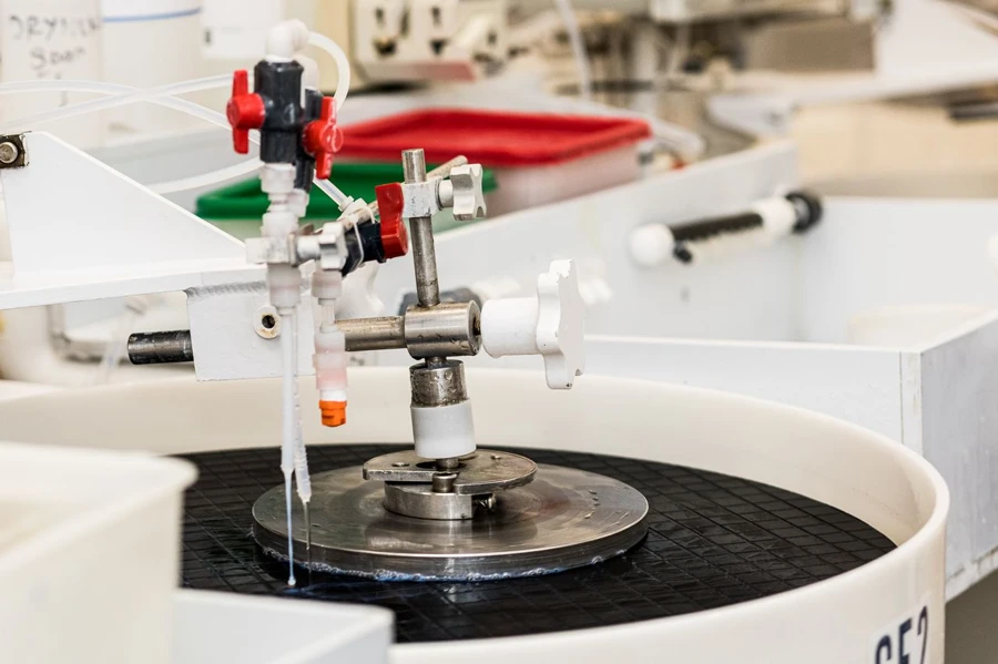
Producing a high-quality GaAs wafer requires careful control throughout the manufacturing process. Even minor inconsistencies can affect electrical performance, reliability, and overall yield. As demand for advanced semiconductor applications grows, manufacturers continue refining production methods to reduce defects and improve consistency across every stage of fabrication.
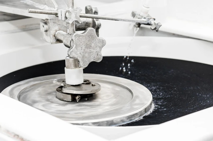
The foundation of wafer quality begins with crystal growth. Producing a stable crystal structure requires precise temperature control, accurate pressure management, and high-purity raw materials. Small variations during growth can introduce dislocations, vacancies, or other imperfections that may affect device performance later in the manufacturing cycle.
A uniform crystal structure is essential for achieving reliable results. Manufacturers must carefully monitor growth conditions to reduce stress within the material and prevent unwanted defects from forming.
Contamination remains one of the most significant challenges in semiconductor manufacturing. Airborne particles, equipment residue, and handling errors can introduce defects that impact production quality.
To minimize contamination risks, manufacturers often focus on:
These measures help maintain cleaner production environments and improve overall manufacturing consistency.
Modern inspection systems play an important role in identifying defects before wafers move into later production stages. High-resolution imaging, automated testing, and detailed surface analysis help manufacturers detect irregularities that may otherwise go unnoticed.
Finding defects early can improve production efficiency, reduce material waste, and support better long-term reliability. Consistent inspection also helps manufacturers identify recurring process issues and implement corrective actions more quickly.
Achieving defect-free production is an ongoing effort. Manufacturers continually evaluate process parameters, equipment performance, and environmental controls to improve yields. Data-driven optimization helps reduce variability while supporting tighter quality standards for advanced semiconductor applications.
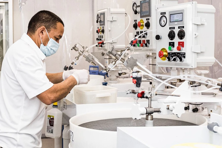
Understanding production challenges is essential when selecting semiconductor materials for demanding applications. If you would like guidance on wafer quality considerations, specifications, or manufacturing requirements, contact us to discuss your project and schedule a consultation regarding your GaAs wafer needs.
Wafer World supports customers with information and solutions for a wide range of semiconductor wafer applications.




