.webp)
During manufacturing, wafers can pass through more than 300 fabrication steps. Silicon wafer processing is a highly precise and detailed procedure, and one single error in any of these steps can render a substrate completely useless.
Nowadays, most defects on wafers are caused by faulty tools. If inspections during the production process don’t capture these, mistakes are carried over multiple steps, only to be discovered at the end, causing millions of dollars in losses. To avoid that, here are some of the most common errors made during wafer manufacturing.
Many wafer manufacturers rely on inspection systems placed on the production lines to identify production defects—if they have any. These systems pinpoint where the problem lies and capture images of it to measure its characteristics, in order to decide the level of damage.
However, as wafers become smaller and thinner, inspection systems are forced to face new challenges. Consider it like this: For bigger surfaces, small defects weren’t considered serious. However, on an ultra thin wafer, even the smallest chip can cause a commotion.
The problem is that as semiconductors continue to shrink, the technology within optical inspection systems hasn’t been able to keep up. The increased demand for wafers leads to a demand for higher production speeds, but if flaws are carried out through the process, entire batches of needed wafers can be rendered useless.
All of this leads to an increasing need for inspection systems with better resolution and accuracy, and higher speeds.
An attractive alternative seems to be automatic detection with machine learning. In fact, many studies are being conducted in that area. However, AI has proven to be effective at identifying defects but not at pinpointing the root of the cause.
This is because defects are often carried over multiple processing steps, so attributing it to one single equipment can be hard. To help you with that, we’ll cover some of the common mistakes during wafer processing, and where they stem from.
The most common defects on silicon wafers are caused by faulty equipment. Here are some of them:
Center-type defects are concentrated around or near the center of the wafer in a circular, ring-like pattern. These defects are commonly called “Bulls Eye” or “Circular ring” defects. They are caused by abnormalities in various equipment:
Local-type defects are concentrated on the edge of the wafer. They don’t exhibit linear or curvy characteristics, unlike scrape type defects.
These defects are scrapes that follow a linear or curvy pattern, distributed from the edge of the wafer, and moving towards the center.
These defects are randomly distributed across the entire surface of the wafer, thus the name.
Something worth noting is that wafers with different defects discovered at the end of the fabrication path are often processed with the same faulty tools. Because of that, it’s common to see a combination of different types of defects on the wafer’s surface.
This only showcases the importance of staying up-to-date in all the manufacturing process, from handling machinery to inspection systems and the production equipment.
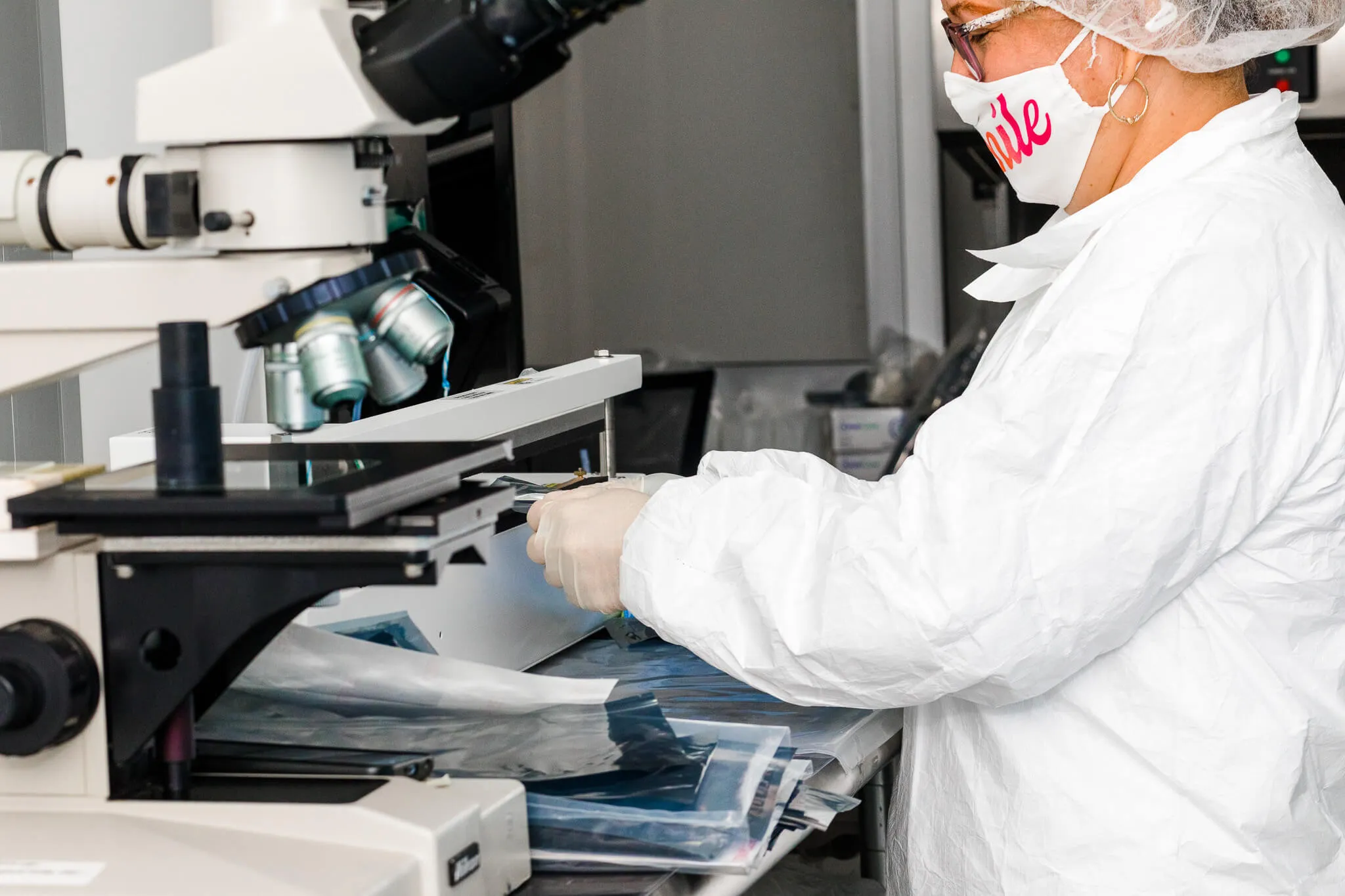
Just as important as identifying faulty equipment is carrying the necessary quality controls for finished silicon wafers. Quality checks identify remaining flaws at the end of the manufacturing process, and ensure wafers are able to meet the industry standards.
Here’s how our quality check looks like here at Wafer World:
.webp)
The world of silicon wafers is constantly changing and innovating. We live in a hyper-digitalized society that depends highly on chips, and other technologies which rely on wafer semiconductors. As the need for these only grows, improving production lines to meet the industry’s demands becomes a must.
However, here at Wafer World we believe increased production must go in line with innovative inspection systems. If these aren’t up to date with production advances, ensuring the quality of wafers becomes impossible.
If you’re interested in seeing how that reflects the quality of our products, call us today to purchase!


