November 2, 2020
Shop NowWe’ve talked a lot about the process for making the silicon wafer (Si wafer), but not nearly enough about why that process is important. At Wafer World, we know exactly why every step of the manufacturing process for silicon wafers is crucial in optimizing their role as a semiconductor and that’s exactly what we will explore.

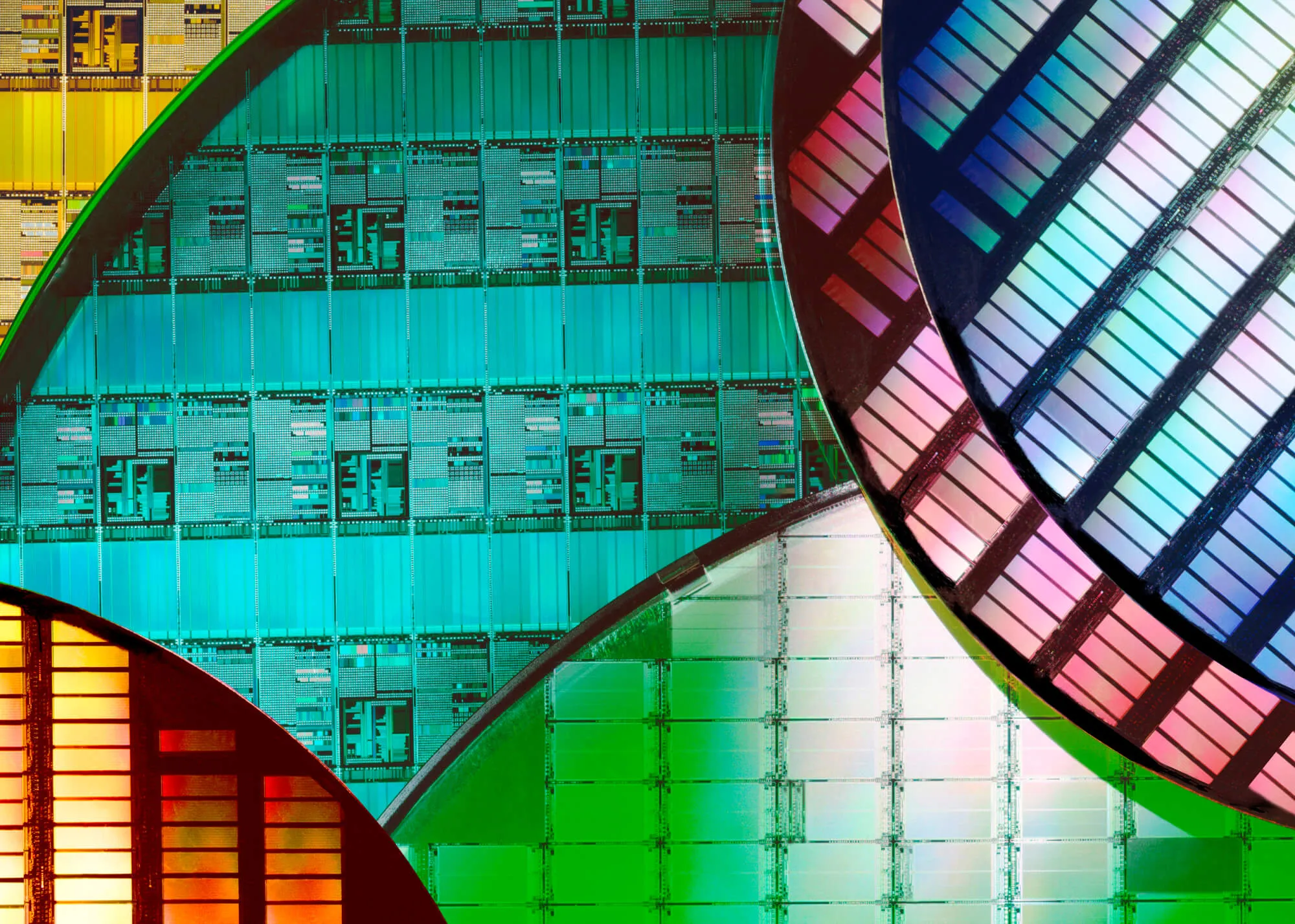
Silicon wafers (also referred to as Si wafers) are slices of semiconductors that are used in the manufacturing process of electronics. Semiconductors can transfer currents at a rate between conductors and insulators, making them ideal for technical processes that require electric currents to be modulated like in computers.
Silicon wafers are all around us and most people don’t realize it. These semiconductors are used in:
The reason the many steps of Si Wafer manufacturing are crucial is because of the way they are used. Silicon wafers are used as semiconductors in integrated circuits, which are essentially multiple circuits connected to a slice (or wafer) of semiconductor material. These components are essential in regulating the flow of electric currents within modern technology. Without them, we would not be able to maintain the efficiency we see in electronics while making them faster and smaller. Because semiconductors are responsible for managing how microscopic particles move from one circuit to another, their purity and overall quality needs to meet the highest standards. Even the tiniest defects at that scale can cause loss of functionality or even substantial damage.
Silicon as it's used in electronics, can’t be found just lying about on the ground, at least not exactly. The silicon used for silicon wafers needs to be extracted from silica sand before it can be refined and turned into Si wafers.
Silica sand contains oxygen that needs to be removed to leave pure silicon. This is done by mixing the sand with carbon and heating it in an electric arc at extreme temperatures. Not only does this process remove oxygen, but other impurities like calcium and aluminum as well.
The reason this matters is because it has everything to do with silicon as an element. Silicon is one of the most abundant elements on planet Earth and although the extraction process is labor-intensive, it’s still more cost-efficient than with other elements. This makes silicon ideal for semiconductor manufacturing.
Once silicon has been extracted from silica sand, it needs to be purified and turned into workable ingots. These are then sliced and turned into the familiar wafer shape we are accustomed to seeing.
There are multiple methods of creating a silicon ingot but the most popular is the Czochralski Process. This method involves melting silicon in a quartz crucible, then rotating it. Then a seed crystal is introduced and rotated in the opposite direction of the molten silicon in the crucible. This causes the silicon to accumulate around the seed crystal which creates an ingot.
The process of making ingots is important for two reasons. First, it helps further purify silicon, which is necessary to limit the amount of interference caused by the material. Secondly, it helps clarify the crystalized structure necessary for optimal conductivity.

After we arrive at silicon ingot that is 99.99% pure, it’s time to cut them into the necessary shape. This is where wafers assume their characteristic appearance and where we determine the thickness necessary for their intended use.
Depending on what the wafers are used for, each slice could have a very different size. To accomplish a precise cut with minimal issues, we use a specialized diamond blade.
Cutting the ingot is essential to getting a wafer closer to its final form. This is the step where the specific requirements of the semiconductor are taken into account.
When a wafer is cut from the silicon ingot, it’s actually a little larger than the needed size. This is because much of the material is removed during the smoothing process, to get to as flat a surface as possible.
The rough wafer adheres to a vacuum which holds it in place before we use equipment to grind minuscule layers from the surface of the wafer. This is done gradually to avoid damaging the wafer.
To the naked eye, after a wafer is sliced it may look pretty flat, but there are tiny imperfections that can cause serious issues if they are not removed. Smoothing gets the wafers one step closer to optimal semiconductor conditions.
Once the surface of the Si wafer has been smoothed, polishing is needed to get to the ideal mirror-like surface. This is one of the final steps of the manufacturing process and the last point at which the wafers lose small layers of material.
We use a combination of chemicals and specialized polishing pads. The wafer is held in place while the pads slowly descend onto the wafer then rise until we get to the smoothest and most reflective surface possible.
Even the smallest of imperfections can hinder the conductivity of silicon wafers. Polishing is necessary to avoid any interference that could impede currents from reaching different circuits.
Wafers need to be spotless to do their job properly. Cleaning the surface is a painstaking but crucial step in making sure these components work how they are supposed to.
We use clean rooms and protective equipment to reduce the risk of any particulates finding their way to the surface of the wafers. Our professionals take a very close look at the Si wafers before giving it the all-clear to enter the testing phase.
Si wafers are responsible for getting particles of unimaginably small size from one place to another. At that small scale, even the tiniest particle can harm the conductivity.
Once the manufacturing is all done, then we need to make sure the wafers work. Testing helps us separate what we can use from what needs to be recycled.
Testing is done by exposing the Si wafers to the real-world conditions they might encounter in practical applications. This includes different electric voltages and high temperatures.
Without semiconductors, the technology you use every day would simply not work. When we turn on the TV or boot up a computer, we expect it to work. Testing is necessary to know that no matter their use, wafers will not be the failing point in any piece of equipment.

At Wafer World, we have a passion for making high-quality products and educating people about a little-understood but unbelievably important aspect of our modern world. Contact us to learn more or request a quote today!


