Ultra-flat wafers are becoming increasingly popular in the semiconductor industry due to their superior surface quality and material properties. However, traditional wafers have been the go-to for many years, making it important to compare and determine which technology is better. In this article, we'll compare ultra-flat wafers to traditional wafers and explore the advantages and disadvantages of each.
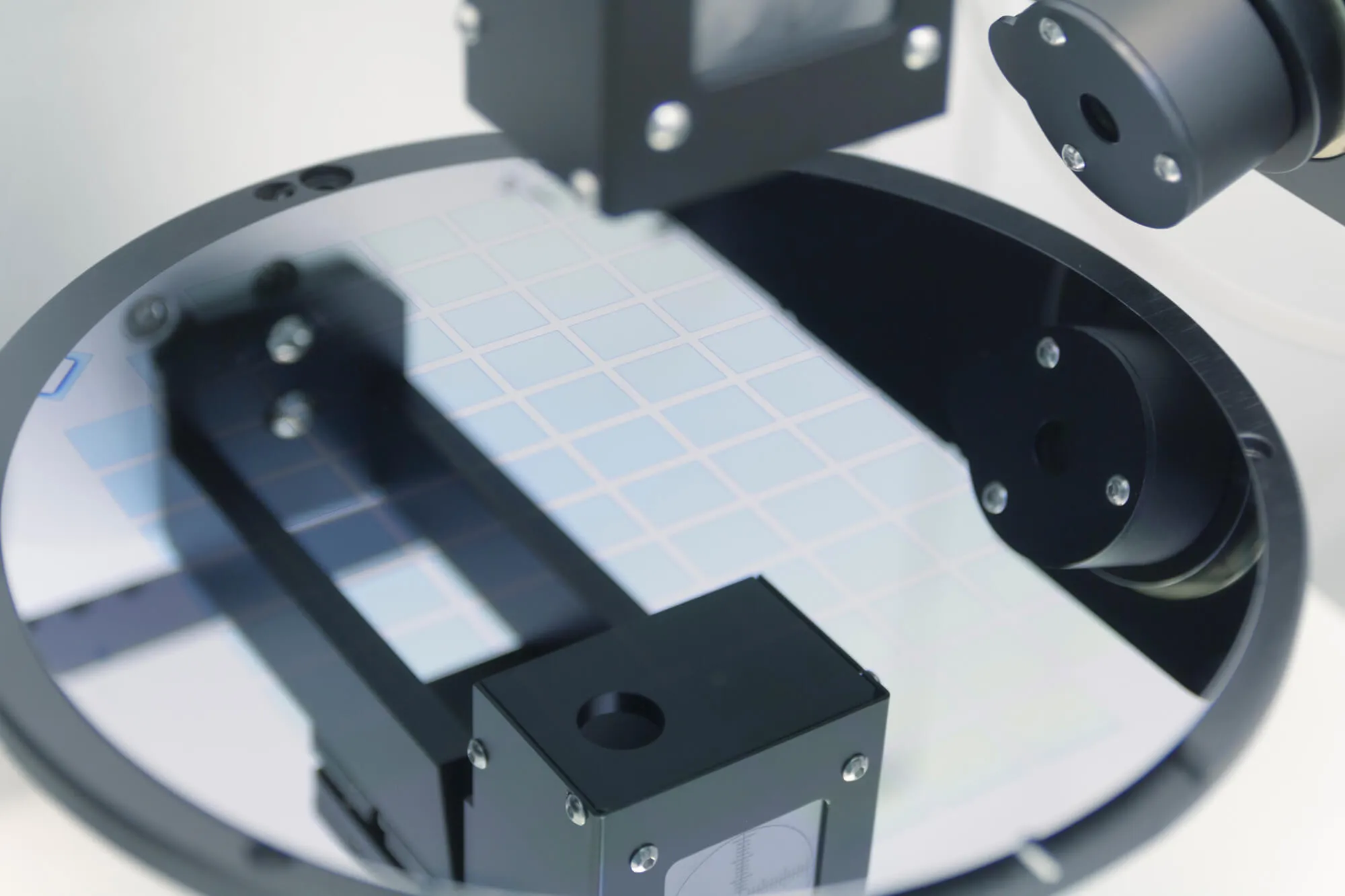
Ultra-flat wafers are characterized by their exceptional surface flatness and material properties. Surface flatness is crucial in wafer processing as it affects the performance of semiconductor devices. Measuring techniques such as atomic force microscopy (AFM) and interferometry are used to assess the surface flatness of ultra-flat wafers. Ultra-flat wafers have a surface flatness of fewer than 0.2 microns, significantly lower than traditional wafers.
The material properties of ultra-flat wafers also make them stand out. They are typically made of silicon or silicon-on-insulator (SOI) and have a low defect density, contributing to their durability and longevity. Ultra-flat wafers are also resistant to thermal expansion, making them ideal for high-temperature applications.
Traditional wafers have been used in the semiconductor industry for many years and are characterized by their surface roughness and material properties. Surface roughness is measured using scanning electron microscopy (SEM) and atomic force microscopy (AFM). Traditional wafers have a surface roughness of around 0.5 microns, significantly higher than ultra-flat wafers.
Traditional wafers are typically silicon and have a higher defect density than ultra-flat wafers. This makes them more susceptible to damage and reduces their durability and longevity. However, traditional wafers are also more flexible and can be made thinner than ultra-flat wafers, making them ideal for flexible applications.
Several factors need to be considered when comparing ultra-flat wafers to traditional wafers. Surface flatness and surface roughness are the most important factors, as they affect the performance of semiconductor devices. Ultra-flat wafers have superior surface flatness, while traditional wafers have higher surface roughness.
Material properties also play a significant role in determining which technology is better. Ultra-flat wafers have a lower defect density and are more resistant to thermal expansion, making them more durable and long-lasting. However, traditional wafers are more flexible and can be made thinner than ultra-flat wafers, making them more suitable for flexible applications.
Overall, ultra-flat wafers have several advantages over traditional wafers regarding surface flatness and material properties. However, traditional wafers are still widely used due to their flexibility and thinner profile. Choosing which technology to use ultimately depends on the application's specific requirements.
%20(1).webp)
Yield rate is the percentage of working devices produced from a batch of wafers. Higher yield rates are desirable because they reduce the number of defective devices and the need for rework, reducing costs and improving delivery times. Ultra-flat wafers can contribute to higher yield rates by reducing defects during the manufacturing process. The ultra-flat surface allows for more precise control of the manufacturing process, reducing the likelihood of defects occurring when wafers are warped or otherwise uneven.
Real-world examples of yield rate improvements due to ultra-flat wafers can be found in various industries. For example, in the display industry, ultra-flat wafers have been shown to improve yield rates by as much as 10% for large panel displays. In the memory industry, ultra-flat wafers have helped to increase yield rates and reduce production costs.
Process control is crucial in semiconductor manufacturing to ensure consistency and reliability. Ultra-flat wafers help to improve process control by allowing manufacturers to more accurately control the thickness and uniformity of the various layers that make up a device. The ultra-flat surface of the wafer enables better control of the deposition of material during the manufacturing process, leading to greater uniformity in the layers that make up the device.
Real-world examples of process control improvements due to ultra-flat wafers can be found in producing advanced semiconductor devices such as transistors and capacitors. In these applications, ultra-flat wafers have helped reduce manufacturing process variability and improve device performance.
Reducing manufacturing costs is a major goal in the semiconductor industry. Ultra flat wafers can help achieve this goal by reducing the number of wafers that need to be scrapped due to defects and by reducing the amount of material required to manufacture each device. By improving yield rates and process control, ultra-flat wafers can help manufacturers to reduce costs and improve profitability.
Real-world examples of cost reductions due to ultra-flat wafers can be found in various industries. For example, in the LED industry, ultra flat wafers have helped to reduce the cost of manufacturing LED chips by up to 20%.
Product performance is a key consideration in the semiconductor industry. Ultra-flat wafers can help improve product performance by providing a more uniform surface for material deposition during the manufacturing process. This leads to devices with greater consistency in their electrical properties, leading to improved performance.
Real-world examples of performance improvements due to ultra-flat wafers can be found in producing advanced semiconductor devices such as solar cells, transistors, and LEDs. In these applications, ultra flat wafers have helped to improve device efficiency and overall performance.
Ultra flat wafers offer a range of benefits to the semiconductor industry. They can help to improve yield rates, process control, reduce costs, and improve product performance. As the semiconductor industry continues to evolve, the importance of ultra-flat wafers will likely grow. Companies that utilize ultra-flat wafers can expect significant improvements in their manufacturing processes and, ultimately, their bottom line.
Ultra-flat wafers are becoming increasingly popular in the semiconductor industry due to their superior surface quality and material properties. They have a lower defect density, are more resistant to thermal expansion, and have exceptional surface flatness. Alternatively, traditional wafers have higher surface roughness but are more flexible and can be made thinner.
Both technologies have advantages and disadvantages, and choosing the right one will ultimately depend on the application's needs. As technology evolves, ultra-flat wafers will likely become even more prevalent in the semiconductor industry.

At Wafer World, our team can help you learn about ultra flat wafers and the process that goes into making them. Get in touch with our team today to get a free quote!


