Double-Side Polished Wafers in Advancing Optoelectronics

Author:

February 23, 2024

Shop Now

In the dynamic realm of optoelectronics, the utilization of advanced materials is pivotal for achieving precision, efficiency, and reliability. One key player in constructing optoelectronic devices is the double-side polish wafer.

This exploration will delve into the critical role that double-side polish wafers play in the realm of optoelectronics, specifically focusing on their applications in LEDs, photodetectors, and optical sensors.

The Essential Role of Double-Side Polished Wafers in Optoelectronics  

The Crucial Foundation: Double-Side Polished Wafers

Light-emitting diodes (LEDs) have become pervasive in various technologies, from cost-effectively illuminating homes to powering advanced display screens with efficiency. Double-side polished wafers form the core for manufacturing high-performance LEDs. The uniformity achieved through double-side polishing is vital for ensuring consistent light emission across the entire LED surface.  

Key Advantages

  • Improved Light Extraction: The smooth surface of double-side polished wafers allows for better light extraction efficiency, maximizing the overall brightness of the LED.
  • Reduced Defects: The polishing process minimizes surface defects, leading to higher yields and improved LED performance.
  • Uniform Thickness: Double-side polishing ensures uniform wafer thickness, contributing to even light distribution in LEDs.

The Precision of Photodetectors

Photodetectors, essential components in devices like cameras and optical communication systems, rely on the precision offered by double-side polished wafers. These wafers provide an ideal substrate for the sensitive photodiodes and sensors that capture and convert light into electrical signals.

Key Advantages

  • Optimized Responsivity: The smooth and defect-free surface of double-side polished wafers enhances the responsivity of photodetectors, allowing them to detect even the faintest light signals.
  • Reduced Dark Current: The meticulous polishing process reduces dark current, improving the signal-to-noise ratio and overall performance of photodetectors.
  • Uniform Light Absorption: Double-side polishing contributes to uniform light absorption across the photodetector surface, ensuring consistent and reliable results.

Optical Sensors: Achieving Precision

Optical sensors, crucial in various applications such as automotive LiDAR systems and environmental monitoring devices, demand a high level of precision. Double-side polished wafers provide the optimal platform for manufacturing these sensors, ensuring accuracy and reliability in data capture.  

Key Advantages

  • High Sensitivity: The smooth surface enhances the sensitivity of optical sensors, allowing them to detect subtle changes in light intensity with greater accuracy.
  • Reduced Signal Noise: Double-side polished wafers contribute to minimizing signal noise, enabling optical sensors to deliver precise and reliable measurements.
  • Improved Signal-to-Noise Ratio: The uniformity achieved through double-side polishing enhances the signal-to-noise ratio, which is crucial for the performance of optical sensors in various applications
double-side-polish-wafer-to-be-polished

Challenges and Innovations in Double-Side Polished Wafers for Optoelectronics

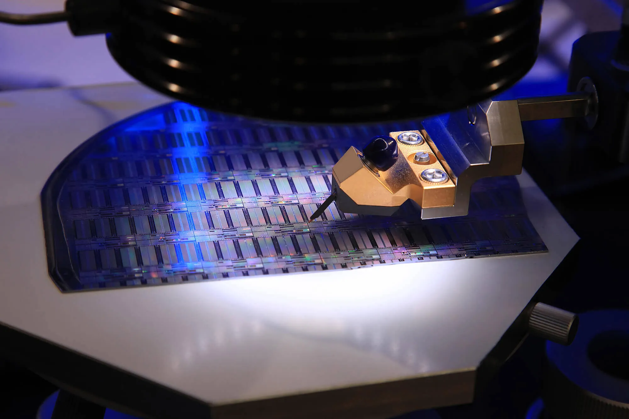
While double-side polished wafers offer significant benefits, the manufacturing process comes with its own set of challenges. Achieving the required surface quality without introducing defects is a delicate balancing act. Innovations in materials and manufacturing techniques have been pivotal in addressing these challenges and advancing them to be more precise and effective.  

Key Innovations

  • Advanced Polishing Techniques: Innovations in polishing techniques, such as chemical-mechanical polishing (CMP), have played a crucial role in achieving superior surface quality in double-side polished wafers.
  • Materials Engineering: Continuous advancements in wafer materials, including silicon and compound semiconductors, contribute to improving the overall performance and reliability of optoelectronic devices.

Future Trends: Larger Wafers and Beyond

As optoelectronic devices continue to advance in complexity and functionality, the demand for larger wafers is on the rise. Larger wafers present both opportunities and challenges in terms of manufacturing precision. The industry is actively exploring innovative solutions to harness the potential of larger double-side polished wafers for even more sophisticated optoelectronic applications to better serve its purpose and increase functionality even more.

Future Trends

  • Transition to Larger Wafers: The optoelectronics industry is gradually transitioning to larger wafers, aiming to increase production efficiency and reduce costs.
  • Integration with Other Technologies: Future trends involve the integration of double-side polished wafers with other emerging technologies, such as AI-driven manufacturing processes and 3D integration techniques.

Collaborative Innovation: A Myriad of Advancements

In the fast-paced world of optoelectronics, collaboration across industries plays a pivotal role in driving innovation. The collaboration between manufacturers of double-side polished wafers and optoelectronic device developers fosters a dynamic exchange of knowledge and expertise, accelerating the pace of advancements in both domains.  

Collaborative Initiatives

  • Joint Research and Development: Collaborative efforts between wafer manufacturers and optoelectronic companies result in joint research and development projects focusing on enhancing the performance and capabilities of optoelectronic devices.
  • Customized Solutions: Manufacturers work closely with optoelectronic device developers to provide customized double-side polished wafers tailored to specific application requirements, further expanding the capabilities of optoelectronics.

Environmental Consciousness: Sustainable Practices in Wafer Production

As industries worldwide increasingly embrace sustainability, the semiconductor industry is also navigating toward greener practices. The production of double-side polished wafers involves intricate processes. Efforts are being made to minimize the environmental impact associated with these manufacturing processes, especially now that companies seek to reduce their carbon footprint to be more sustainable and eco-friendly.

Sustainable Practices

  • Recycling Initiatives: Wafer manufacturers are exploring recycling initiatives to minimize waste generated during the production of double-side polished wafers.
  • Energy-Efficient Manufacturing: Implementing energy-efficient manufacturing processes contributes to reducing the carbon footprint associated with wafer production.
  • Materials Selection: Opting for environmentally friendly materials and manufacturing chemicals in the wafer production process is becoming a focal point for sustainable practices in the semiconductor industry.

The Road Ahead: Charting the Course for Optoelectronics

The journey of double-side polished wafers in the realm of optoelectronics is dynamic and ever-evolving. As the demand for high-performance optoelectronic devices continues to rise, the role of double-side polished wafers becomes increasingly pivotal.

Whether in the realm of quantum dots, silicon photonics, or collaborative industry initiatives, these wafers are the unsung heroes, contributing to the precision, efficiency, and sustainability of the optoelectronics landscape.

double-side-polish-wafer-to-be-polished

Order Double-Side Polish Wafers Today!  

The intricate dance of technology and materials science is illuminated by the precision and versatility of double-sided polished wafers. As we navigate quantum advancements and collaborative innovations, the symbiotic relationship between these wafers and emerging optoelectronic technologies ensures a future where light and data converge with unprecedented precision and efficiency.

The road ahead for double-side polished wafers from Wafer World is not easy, but it is shaping the future of optoelectronics for everyone’s benefit. Contact us to order!

Wafer World Banner