April 27, 2026
Shop NowThe electronics industry has always been shaped by one central goal: doing more with less. Devices are expected to be smaller, lighter, faster, and more energy-efficient than ever before, all while delivering reliable performance in increasingly demanding environments. That shift has pushed manufacturers to rethink the materials and structures used at the heart of modern devices. One of the most important developments in that effort is the move toward thin silicon wafers, which support compact designs without sacrificing functionality. As production methods improve and applications expand, these advanced wafers are becoming a major force behind the next generation of electronics.
For many years, thicker wafers served as the standard foundation for semiconductor manufacturing. They offered durability during handling and processing, which made them practical for traditional fabrication environments. As electronics evolved, however, older wafer formats began to create limitations. Larger and heavier materials could only support miniaturization to a point, which became a challenge as manufacturers worked to produce slimmer phones, lighter wearables, and more efficient industrial components.
The shift away from bulkier structures did not happen overnight. It required advances in slicing, polishing, handling, and inspection to ensure that reduced thickness would not compromise performance. What began as a technical challenge has now become a major advantage. Thinner materials allow engineers to rethink product design from the ground up, giving them greater flexibility in arranging circuits, sensors, and components within limited space.
In electronics, size affects more than appearance. It influences heat management, energy use, packaging efficiency, and overall device behavior. A reduction in wafer thickness can support lighter and more compact systems, which is especially valuable in products designed for portability or dense integration. This matters in markets where every millimeter of space has value.
Thinner structures can also improve thermal performance when combined with the right design strategies. Managing heat is critical in electronics because excessive temperature can shorten component life and reduce consistency. Materials that fit into more optimized layouts make it easier for designers to build systems that perform well under real-world conditions.
Another important factor is responsiveness. Devices that process information quickly rely on highly refined structures and carefully engineered pathways. When materials are adapted to smaller, more efficient architectures, they help support the speed and precision modern electronics require.
Compact design is no longer a premium feature. In many industries, it is the baseline expectation. Consumers want devices they can carry easily, businesses want systems that use space efficiently, and industrial applications often require compact performance in constrained environments. Thinner wafer technology supports all of these goals by helping reduce the physical footprint of critical components.
This makes a difference in products such as smartphones, tablets, wearable monitors, and smart home devices. It also supports more advanced tools used in telecommunications, medical systems, and automotive electronics. When device manufacturers can build smaller devices without giving up power or reliability, they gain a stronger position in a highly competitive market.
The benefits are not only external. Smaller internal architectures often create opportunities for better organization inside the device itself. That can improve airflow, simplify assembly, and support a more efficient arrangement of supporting components.
The influence of ultra-thin wafer development reaches well beyond consumer products. In automotive electronics, compact, efficient components are essential for sensors, control systems, and advanced driver-assistance systems. These systems need to perform consistently under varying temperatures and conditions, so material quality and design precision matter greatly.
In medical technology, smaller components can support less invasive devices, portable diagnostic tools, and more convenient monitoring systems. That combination of reliability and compactness is especially important in settings where performance can directly affect care and outcomes.
Industrial electronics also benefit from reduced material thickness when operating in tight spaces or under continuous use. From monitoring equipment to automation platforms, design efficiency helps manufacturers improve both functionality and long-term value.
Aerospace and defense applications can also benefit from lighter and more compact electronics, where space and weight are often limited. In these demanding settings, efficient material solutions can support both performance goals and structural priorities.
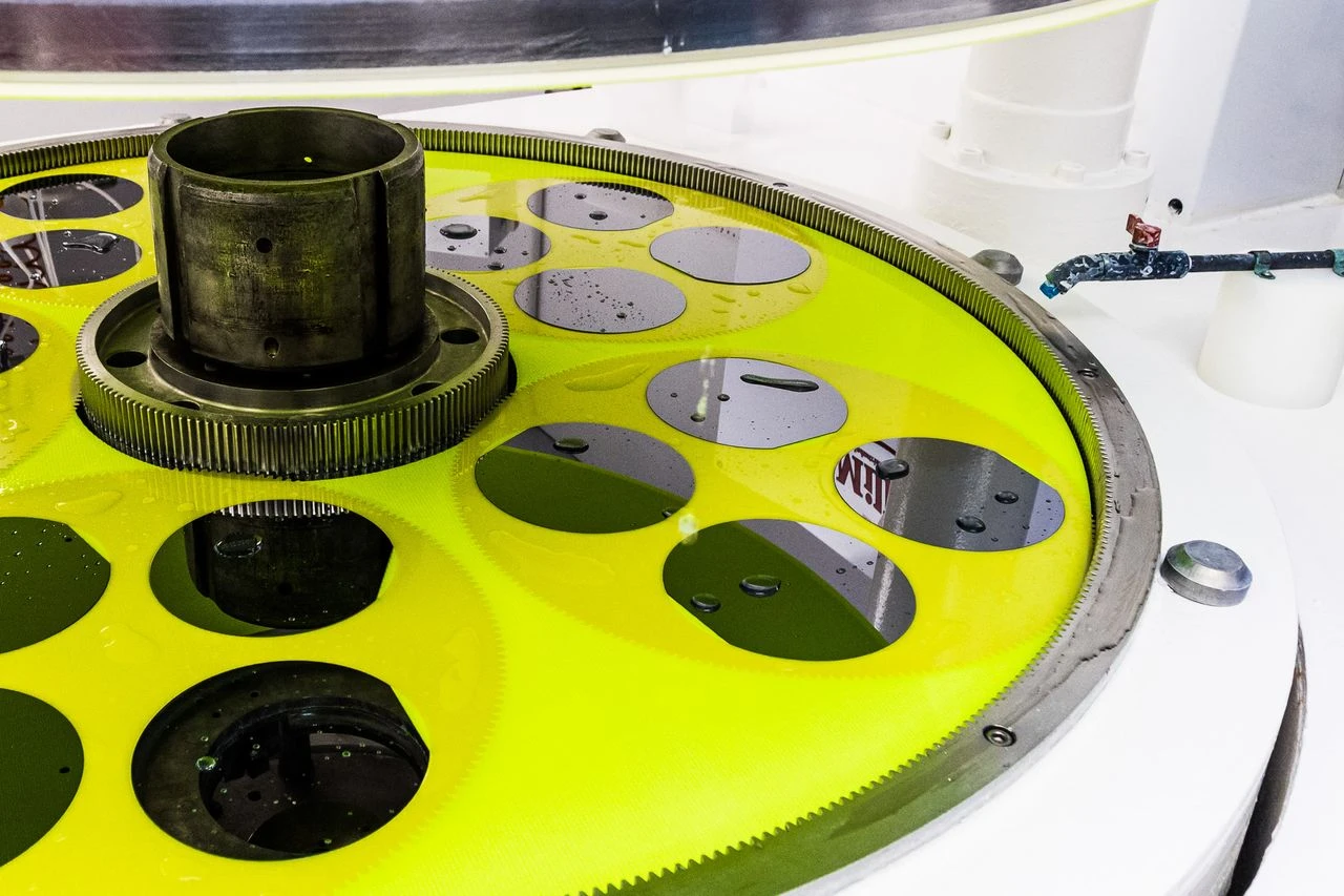
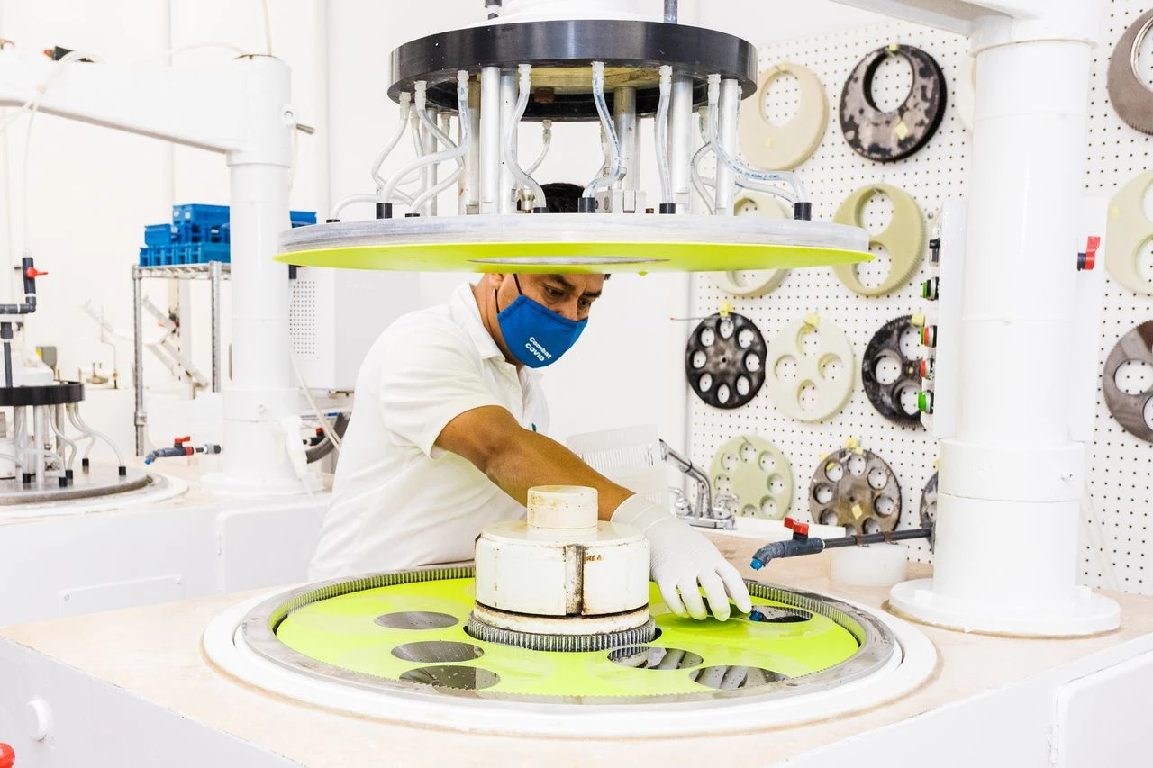
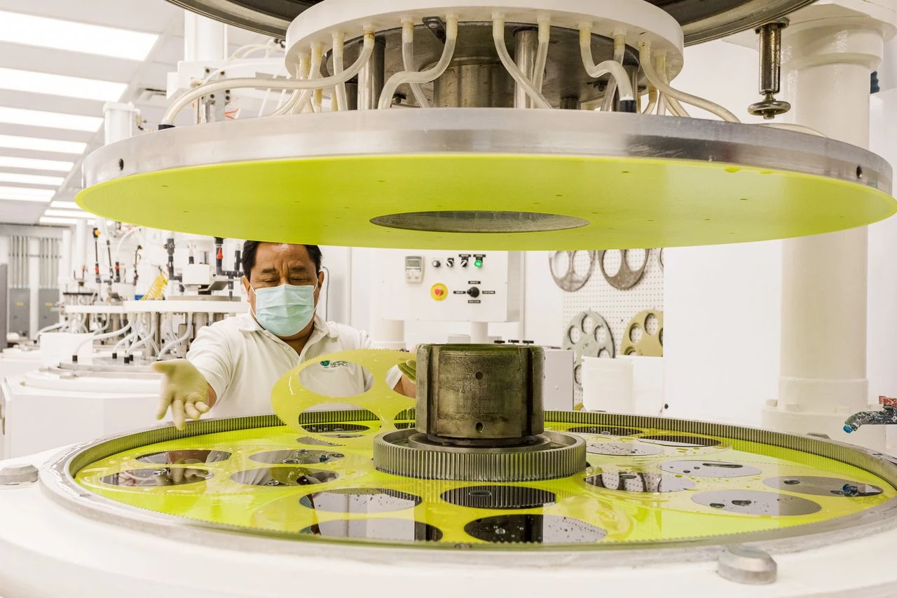
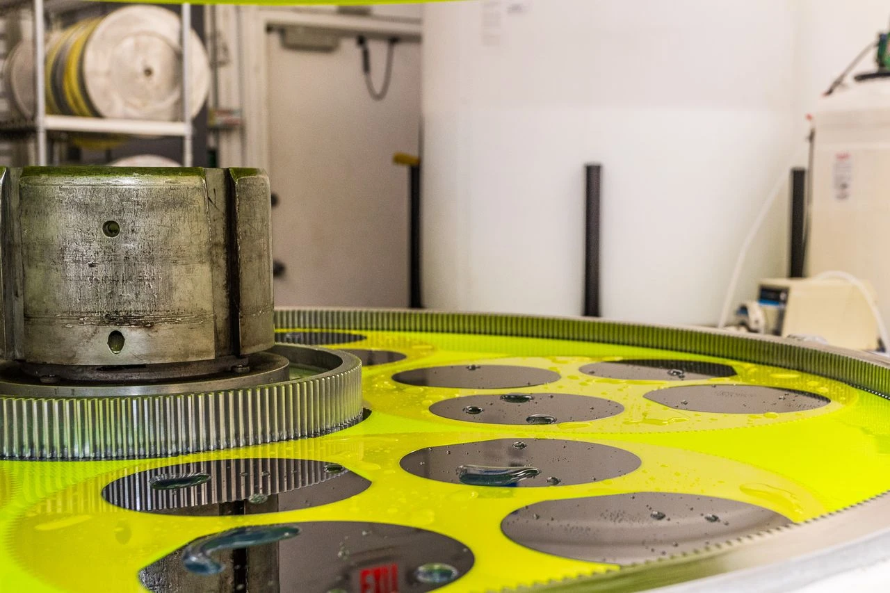
None of these benefits would matter without precise manufacturing. Producing thinner wafers requires careful control at every stage, from material preparation to slicing, polishing, and finishing. Even small inconsistencies can affect flatness, handling, and downstream performance, so quality standards must remain high throughout the process.
Manufacturers rely on refined techniques to ensure each wafer meets exact thickness and surface requirements. Consistency is especially important when the final product will be used in sensitive or high-performance applications. A well-produced wafer supports better fabrication outcomes and reduces the likelihood of defects later in the production cycle.
Handling is another major consideration. As materials become thinner, the processes of transporting and processing them must be carefully managed. This has led to broader improvements in manufacturing systems, inspection methods, and support technologies that help preserve quality while maintaining efficiency.
As electronics continue to evolve, wafer technology is helping open the door to new product types and capabilities. Flexible systems, smart sensors, and highly integrated platforms all depend on materials that enable precision in smaller, more adaptable formats. This is especially relevant in emerging categories where comfort, portability, and energy-conscious design are major priorities.
The continued development of more advanced wafer formats also encourages innovation at the design level. Engineers can test new layouts, rethink packaging strategies, and create products that better respond to user needs. In that sense, wafer development is not just keeping up with innovation. It is helping drive it.
This long-term impact is one of the reasons thinner wafer solutions matter so much. They support the immediate needs of today’s electronics while also creating opportunities for what comes next. As demand rises for devices that are more capable without becoming larger or heavier, material innovation will remain central to the conversation.
As electronics continue moving toward smarter, smaller, and more efficient designs, choosing the right material foundation becomes even more important. Thin silicon wafers can help improve performance, enable better integration, and enable more flexible product development across a wide range of applications. At Wafer World, we provide dependable wafer solutions built for precision and consistency, helping you move forward with confidence. Contact us today to explore options that align with your technical goals and support your next stage of innovation.


