Did you know that a GaAs wafer generates less noise than other wafers? This is just one simple advantage of GaAs material intertwined within a wafer. Let’s keep reading to learn more about what GaAs is and the advantages you need to know!
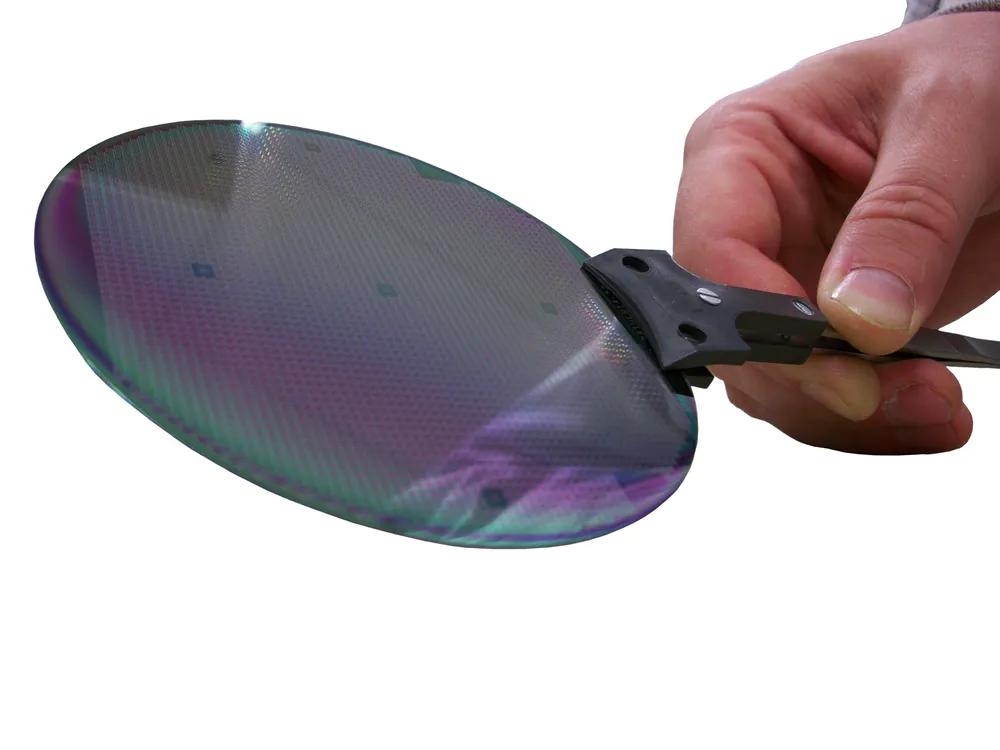
Gallium Arsenide (GaAs) is a great semiconductor composed of the element Gallium (Ga) and Arsenide (As). After melting metals such as aluminum, Gallium is created as a direct result. Arsenic is an elemental crystal that can be found in other minerals such as metals. GaAs wafers can range from 1 in. to 11 in.
There are many advantages associated with a GaAs wafer including:
Moreover, since the GaAs compound is not fazed by heat, this makes it a great semiconductor that does not overheat.
In addition, GaAs wafers are typically found as an application as an integrated circuit in field-effect transistors. They are useful for high radio frequencies and electronic switching purposes. If amplification of material is too weak, GaAs wafers are ideal for the cause.Furthermore, GaAs wafers have a high range of free electrons that serve as the perfect environment for circuits and devices. As a result, this electron gap makes way for photon production in LEDs and high-powered laser devices.

Last but not least, we know the importance of getting a GaAs wafer that will provide significant benefits for the semiconductor industry. At Wafer World, we are committed to crafting and supplying our customers with highly optimized wafers. GaAs is an ideal compound that has become more common in recent years. Contact us today to learn more about our wafers!


