Modern CPUs and computer chips power everything from smartphones to data centers—but the process behind their creation is one of the most complex manufacturing workflows ever developed. One of the most overlooked—but absolutely critical—factors is wafer preparation, particularly the use of a double side polish wafer.
Procuring the wrong type of double-sided polish wafers can easily determine success or failure at scale when manufacturing CPUs—for this reason, understanding how CPUs are manufactured—and how wafer flatness, surface quality, and polishing directly impact performance, yield, and cost—is fundamental for achieving better outcomes.
Every CPU starts as a digital blueprint. Engineers design billions of transistors using Electronic Design Automation (EDA) software, defining logic, memory, and interconnect layers at the nanometer scale.
At this stage:
This is why the mechanical stability of the wafer becomes crucial long before fabrication even begins.
Once the design is finalized, it’s transferred to photomasks—high-precision templates used during the lithography process. Each CPU may require dozens of masks, one for every layer. Any distortion in wafer geometry during exposure can cause:
To avoid this, flat, stress-free wafers are essential for accurately reproducing these mask patterns across the entire surface.
This is the foundation of the entire process.
The previously crafted designs and masks need to be then etched into a silicon wafer, which will act as the substrate for the chip. Making a silicon wafer begins by growing high-purity silicon crystals, typically using the Float-Zone method, as this process can result in purer silicon with less oxygen contamination.
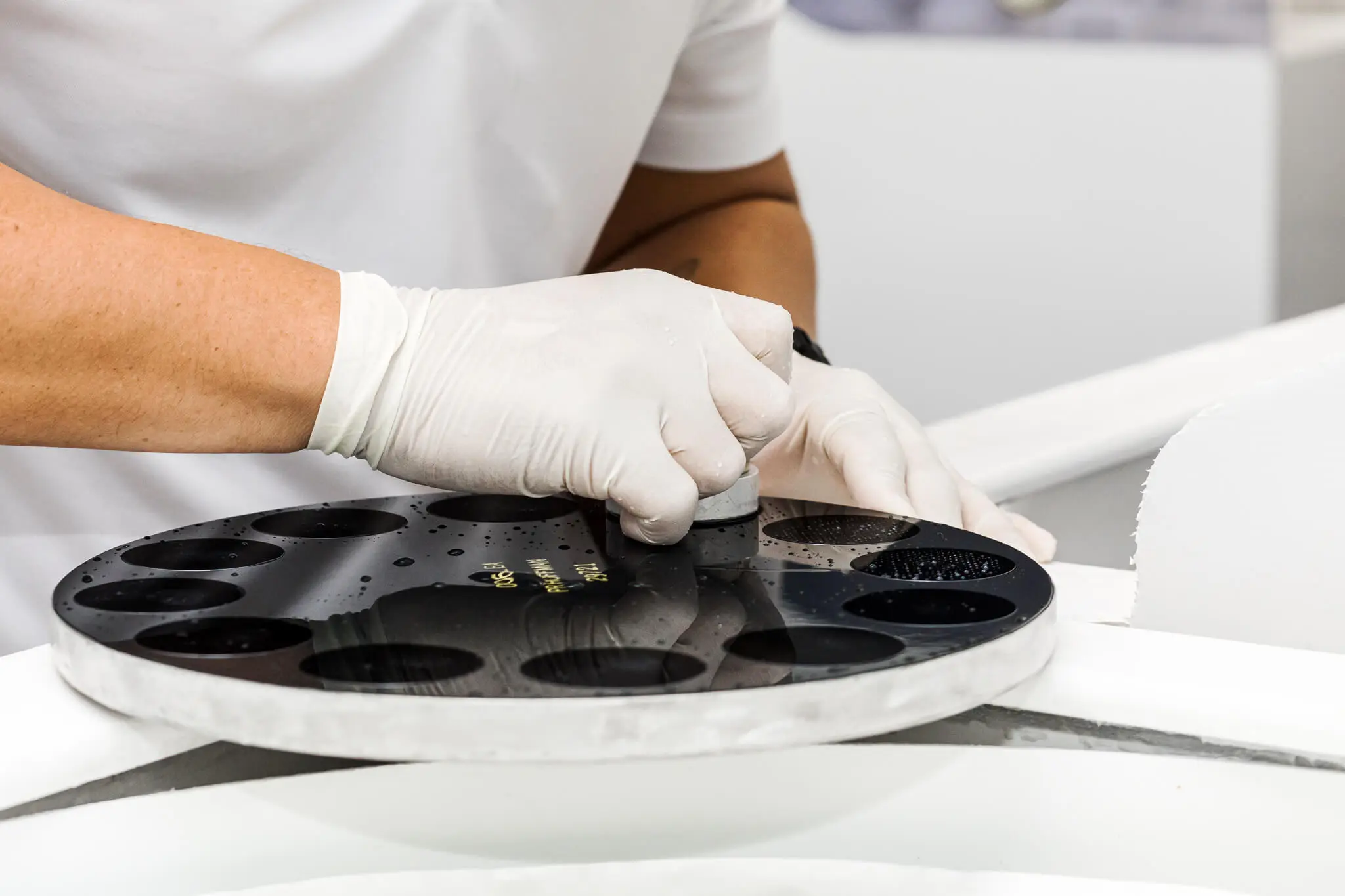
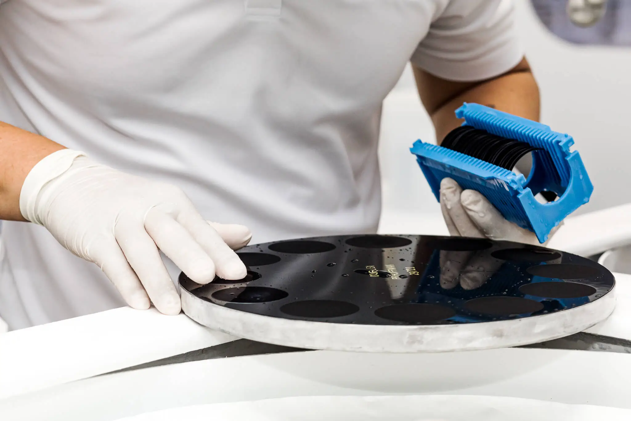
The ingot is then sliced into thin wafers, which are lapped, etched, and polished to achieve a smooth surface.
A double-sided polished wafer is polished on both the front and back surfaces, unlike single-sided polished wafers, which leave the backside rough.
For advanced CPU manufacturing, DSP wafers ensure an improved overlay accuracy and less focus variation during lithography. They also enable thinner wafers without breakage, increasing overall yield and process repeatability. This is why double-sided polish wafers are standard in advanced logic, test wafers, and reclaim wafer applications.
Once the silicon wafer has been prepared, the next phase involves building ultra-thin material layers that will later form the functional components of the CPU.
This is achieved through a range of thin film deposition techniques, each selected based on the electrical, chemical, and structural properties required. Precisely controlling film thickness at the atomic level, manufacturers form insulating layers, gate oxides, and conductive paths that define the behavior of transistors.
At this stage, wafer geometry becomes critically important. Even minimal bowing or warping can lead to uneven material coverage, resulting in variations in electrical performance across individual dies. Double-sided polish wafers play a key role in preventing these issues by maintaining superior flatness across the entire surface.
Photolithography is the process that transfers intricate circuit patterns from a photomask onto the wafer using light. It usually goes as follows:
Double-sided polish wafers provide a significant advantage here by sitting flatter on vacuum chucks, minimizing local height variations, and enabling more consistent critical dimension control.
Following photolithography, etching is used to remove unwanted material and permanently define the circuit structures. Depending on the materials involved, manufacturers may use dry plasma-based etching or wet chemical etching to carve features into the deposited layers selectively.
The goal is to replicate the photolithographic pattern with absolute fidelity, preserving feature size and depth across the wafer. Double-sided polish wafers help ensure uniform etching conditions across every die, improving pattern accuracy and maximizing functional yield throughout the wafer.
Ion implantation is used to precisely introduce dopant atoms into the silicon lattice, allowing manufacturers to control the electrical conductivity of specific regions within the transistor. This process involves accelerating ions toward the wafer surface at high energy, embedding them at controlled depths and concentrations.
Because of the energies involved, implantation is highly sensitive to wafer orientation, surface uniformity, and mechanical stability. Any backside roughness or wafer bow can disrupt the implantation angle or beam uniformity, leading to uneven dopant distribution, channeling effects, or device mismatches.
Double-sided polish wafers mitigate these risks by providing a smooth, polished backside that enhances electrostatic clamping and stabilizes the wafer during implantation. This results in more uniform dosing, improved device consistency, and tighter control over transistor performance.
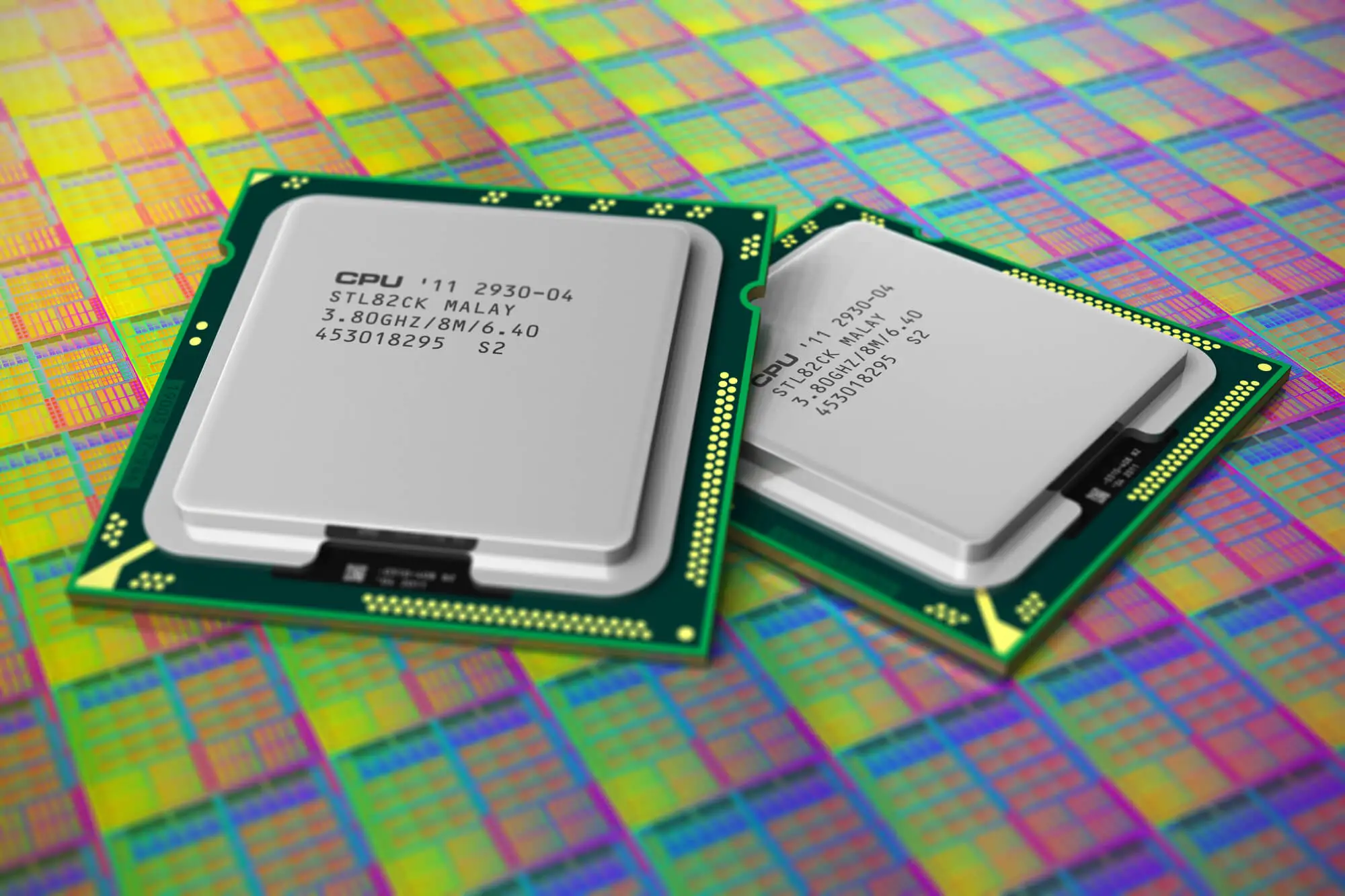
Once the transistors are formed, metallization is used to connect them into functional circuits electrically. Modern CPUs rely on highly complex interconnect architectures that may include more than ten metal layers stacked vertically, often arranged in three-dimensional configurations to maximize performance and density.
Each new metal layer adds mechanical stress to the wafer, increasing the risk of distortion over time.
Double-sided polish wafers help manage these cumulative stresses by minimizing warpage and maintaining structural integrity throughout repeated processing cycles. Their enhanced flatness reduces the likelihood of delamination between layers and ensures consistent alignment from the first metal layer to the last.
Before individual chips are packaged, completed wafers undergo electrical testing to verify functionality and identify known-good dies. Probing systems make direct contact with each die to measure performance, after which the wafer is mapped and prepared for separation.
The wafer is then diced into individual chips, which are assembled into packages and prepared for final testing and evaluation.

CPUs are marvels of engineering, but they’re only as good as the surface they’re built on. From lithography to implantation to packaging, double side polish wafers quietly enable the precision modern chips demand.
Do you need double side polish wafers for your next project? Wafer World can help. Choosing the right double side polish wafer supplier can directly impact performance, yield, and long-term success. Reach out and experience the benefits of our DSP wafers!


