In the production of semiconductors and chips, laser marking is now a crucial stage. Laser marking guarantees that each chip can be accurately identified without sacrificing performance, whether for traceability, quality control, or regulatory compliance. We'll examine the technologies involved, dissect how laser marking for chips operates, and discuss why it's revolutionizing the semiconductor industry in this guide.
Permanent identifiers, such as serial numbers, 2D codes, or logos, can be directly applied to semiconductor wafers, IC chips, or packaging materials using laser marking, a non-contact technique. In contrast to mechanical or ink-based techniques, laser marking modifies the material's surface with concentrated light energy to create accurate, long-lasting marks.
For semiconductor chips, laser marking is critical because it allows manufacturers to:
Semiconductor manufacturing involves hundreds of steps, often across multiple locations and suppliers. Without reliable marking, it’s nearly impossible to trace production issues, manage recalls, or ensure proper assembly.
With laser marking, you can ensure that each chip has a unique identifier, enabling manufacturers to track it from wafer to finished product. By confirming that every chip has passed inspection and meets the requirements, this also aids in quality control.
Due to its advantages, laser marking has become fundamental to meeting various industries’ compliance regulations, especially in sectors such as automotive, aerospace, and medical. Lastly, laser markings are difficult to remove, which helps prevent counterfeiting and ensures authenticity.
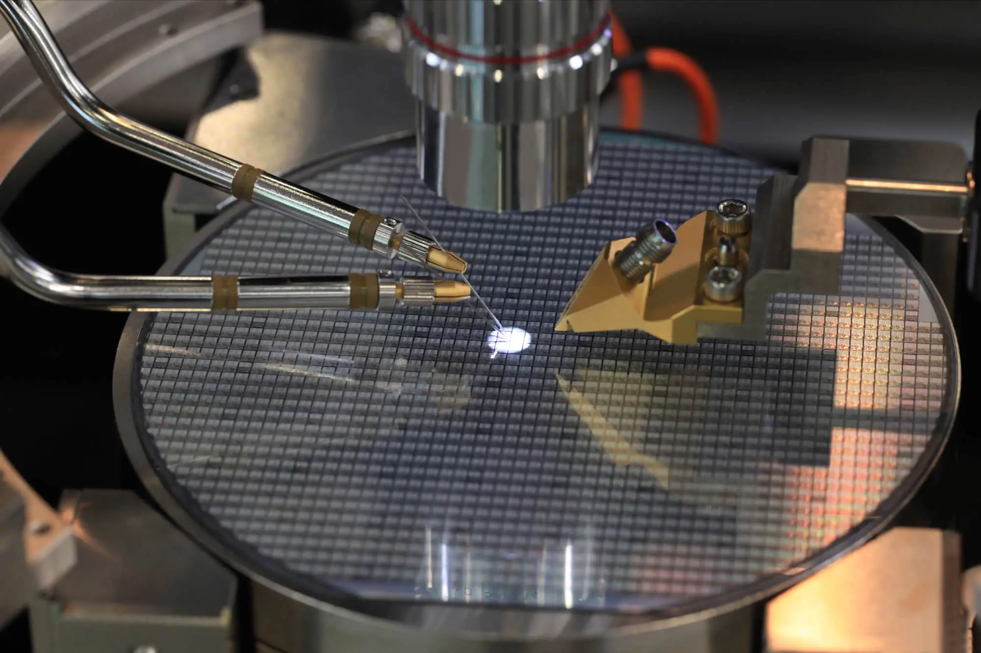
At its core, laser marking uses a highly focused beam of light to interact with the surface of a chip or wafer. Depending on the material and desired effect, the laser can etch the surface by vaporizing a small layer of material, anneal the surface, or foam or discolor certain polymers used in chip packaging.
The process typically involves:
Different laser types are used depending on the material and marking requirements:
Fiber lasers are ideal for metals and semiconductor substrates. They produce highly precise marks with minimal heat-affected zones. For that reason, they’re commonly used in IC chips and wafer edge marking.
These are excellent for delicate substrates and polymer packaging. UV lasers produce clean, high-contrast marks without damaging sensitive circuits. They’re widely used in microelectronics and MEMS devices.
Primarily used for marking plastics and non-metallic packaging, CO2 lasers provide high-speed marking for mass production.
Laser marking offers several benefits that make it ideal for semiconductor manufacturing, such as:
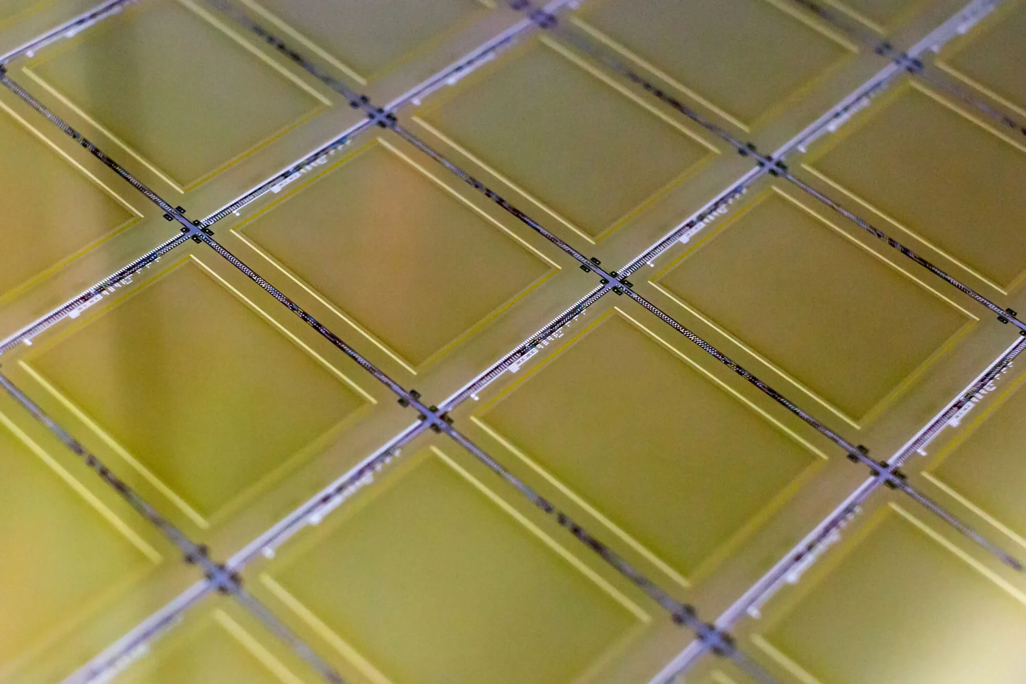
Before chips are separated (dicing), wafers are marked with batch numbers, manufacturing dates, and process codes. This ensures traceability from wafer to finished IC.
After dicing, individual chips may receive:
Laser marking can also be applied to chip packaging or modules, ensuring all components are traceable and authenticated throughout the supply chain.
By marking chips before and after testing, manufacturers can identify defective units, correlate failures with production batches, and prevent defective chips from reaching customers.
When selecting a laser marking system, there are various factors worth considering, such as:
Are you still in doubt about the benefits of wafer marking? Here are some frequently asked questions, along with their answers.
Fiber UV and CO2 lasers are widely used depending on the material and precision requirements.
It is non-contact, more precise, permanent, and compatible with delicate semiconductor materials.
When properly configured, laser marking does not impact chip functionality or reliability.
Laser systems can be integrated with MES and vision inspection tools for real-time tracking and quality control.
Yes, it eliminates the need for inks, solvents, or physical consumables, reducing waste and chemical exposure.
Laser marking is no longer just an optional step in semiconductor manufacturing—it’s a cornerstone of traceability, quality control, and efficient production. By using non-contact, high-precision lasers, manufacturers can mark chips safely, durably, and quickly, ensuring every component is tracked from wafer to end device.
For electronics manufacturers, finding providers that incorporate laser marking is crucial. At Wafer World, we recognize the importance of this step in enhancing traceability, minimizing contamination risks, and future-proofing production lines. If you’d like to learn more about our laser marking methods, reach out!


