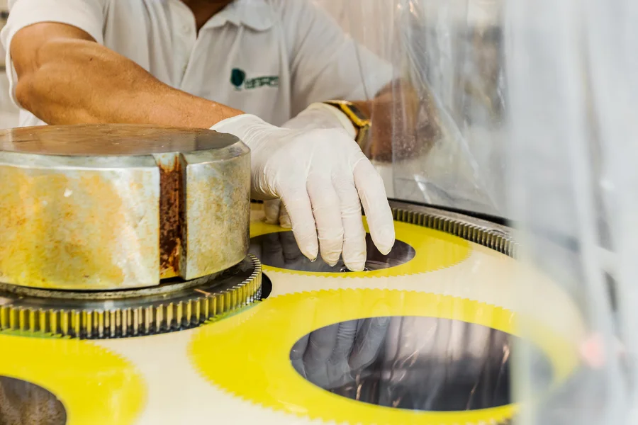
Semiconductor processes do not always leave a substrate ready for another trip through fabrication equipment. Films, residues, surface damage, and other changes may remain after a wafer has served its original purpose. Producing GaAs reclaim wafers involves determining whether used gallium arsenide substrates can be prepared for another appropriate application, then addressing their surface condition through carefully controlled processing.
Reclaiming is therefore better understood as a qualification and restoration workflow rather than simply a cleaning procedure.
The process starts before any material is removed. Incoming wafers need to be examined to identify unsuitable substrates rather than automatically entering the reclaim workflow.
This distinction matters because polishing cannot correct every type of damage. A substrate may have chips, cracks, deep scratches, or dimensional characteristics that make further processing impractical for its intended use. Previous processing may also have deposited films or created surface changes that require specific removal methods.
An incoming inspection provides a baseline for deciding what the substrate needs. The exact criteria depend on the reclaim process and intended application, but the evaluation may consider:
The purpose is not to assume that every used substrate can be recovered. It is to determine which wafers are reasonable candidates for further processing.
A previously processed GaAs substrate may carry deposited material that must be removed before the underlying surface can be refinished. Depending on what is present, material removal can involve chemical or mechanical techniques designed around the specific layers on the wafer.
Research involving GaAs demonstrates how selective wet etching can remove semiconductor material within carefully designed structures. A NIST-published study, for example, describes selective wet etching of GaAs relative to AlGaAs during substrate-removal work. While this research was not a commercial reclaim procedure, it illustrates an important principle: material-removal chemistry must be selected according to the materials present and the desired result.
More aggressive removal is not automatically better. The objective is to eliminate unwanted material while preserving sufficient substrate for subsequent preparation.
That makes process control important. Chemical exposure, mechanical action, and the amount of material removed can influence the condition and dimensions of the remaining wafer. The reclaim sequence, therefore, needs to consider the substrate that must remain after stripping, not only the layer that must be removed.
Once unwanted layers have been addressed, the wafer surface may require mechanical or chemical-mechanical refinement. These operations can remove affected surface material and produce a smoother working surface.
Historical NASA research on GaAs processing evaluated different polishing sequences after lapping. The researchers found that polishing methods produced varying levels of surface defects and noted that a two-step chemical-mechanical polishing sequence after lapping yielded better wafers more consistently in their experimental setup.
This finding highlights why polishing should be treated as a controlled manufacturing operation rather than a cosmetic step.
A scratch that is easy to see is only one type of concern. Mechanical preparation can cause subsurface damage that may not be apparent during routine visual inspection.
NASA research using X-ray topography on GaAs found that surface damage could affect observations of crystal imperfections. In one experiment, chemical polishing exposed deeper irregularities associated with earlier surface damage instead of simply producing the expected flat surface.
For reclaim processing, this reinforces the importance of carefully evaluating the substrate. A shiny appearance alone does not prove that the surface has reached the condition required for another application.
Every material-removal step has a consequence: the substrate becomes thinner. This is one of the fundamental limits on how a used wafer can be restored.
A reclaim process may remove coatings, damaged surface material, or other layers before the final finish is achieved. The resulting wafer must still satisfy the dimensional requirements of its intended application and be compatible with the equipment that will handle it.
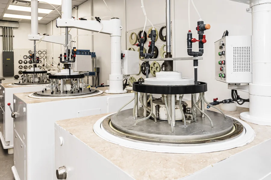
This is why the number of times a substrate can potentially be processed should not be treated as a universal figure. The starting thickness, amount of material removed, existing damage, final dimensional requirements, and previous history can all influence whether another reclaim cycle is reasonable.
The current specification is more useful than assumptions based on the wafer’s original dimensions. After processing, measurement helps establish what the substrate has become and whether it remains appropriate for its next task.
Polishing and stripping can leave residues of their own. Particles, polishing compounds, chemicals, and material removed from the surface should not remain on a prepared wafer.
Historical NASA documentation for preparing epitaxial GaAs wafers describes multiple cleaning and rinsing operations around polishing, including steps intended to remove dust, mounting residues, oils, and polishing compounds before further surface preparation.
Modern reclaim workflows may differ substantially from those historical research procedures. Still, the underlying lesson remains relevant: surface restoration and cleaning are connected processes.
Cleaning should be matched to the materials involved and the required final condition. A wafer that has been polished but retains unwanted residue has not completed the preparation needed for a cleanliness-sensitive application.
After surface restoration and cleaning, the substrate needs to be evaluated again. Incoming inspection asks whether a wafer is a candidate for reclaim. The final inspection asks whether the processed substrate meets the applicable acceptance requirements.
This stage may involve dimensional measurements, surface inspection, or other tests appropriate to the specification. The exact measurements depend on what the customer or downstream process requires.
A reclaimed wafer should not be assumed to be identical to a newly manufactured substrate. Reclaiming has removed material, and the wafer has a prior processing history.
A more useful question is whether the finished substrate meets defined requirements for its next use. Clear specifications give suppliers and users a common basis for making that decision.
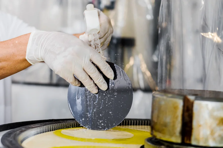
Reclaimed substrates can be considered for applications where their resulting specifications are appropriate. Potential use should always be determined by the actual wafer condition and process requirements, rather than by the reclaimed label alone.
Some semiconductor operations may place especially demanding requirements on crystalline quality, surface condition, electrical properties, or epitaxial readiness. Other activities may prioritize dimensions, handling compatibility, or a prepared surface for process development.
Understanding that distinction helps prevent two opposite mistakes: assuming reclaimed material is suitable for everything or assuming it has no place in advanced semiconductor environments.
No. Cleaning can be one part of a broader reclaim workflow. Reclaim processing may also require incoming inspection, removal of previous films, surface material removal, polishing, dimensional evaluation, and final qualification. The exact sequence depends on the substrate’s condition and intended reuse.
Not necessarily. Damage, insufficient remaining thickness, edge condition, previous processing, or other characteristics may make a substrate unsuitable for a particular reclaim process or future application. Qualification should occur before restoration work begins.
Polishing can help remove affected surface material and create a smoother surface. Research on GaAs preparation also shows that polishing methods can influence scratches, surface damage, and final surface characteristics, making process selection important.
Material-removal operations can reduce thickness. The amount depends on the wafer’s initial condition and the processing required. Current dimensional measurements are therefore important when evaluating whether the finished substrate is suitable for another use.
There is no single test that establishes suitability for every application. Evaluation can involve checking dimensions, edge integrity, surface condition, cleanliness, and other specifications relevant to the next process. Acceptance requirements should be defined according to the intended use.
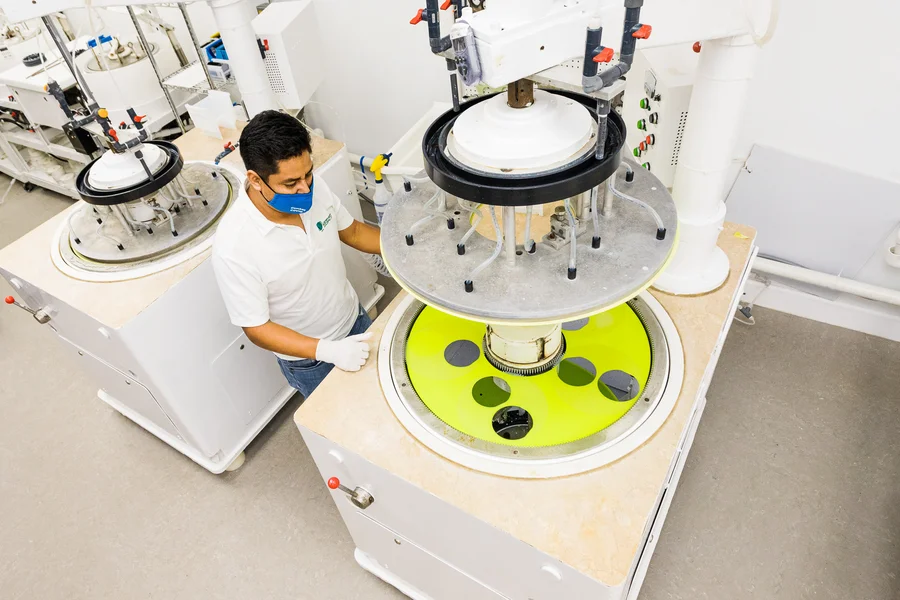
If GaAs reclaim wafers are part of your sourcing or substrate-reuse plans, start by identifying the dimensions, surface requirements, condition, and intended application that matter to your process. Wafer World can help you review available material and discuss specifications without assuming that every reclaimed substrate fits the same purpose.




