April 22, 2026
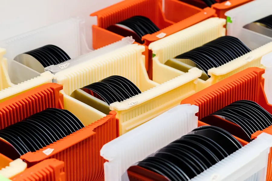
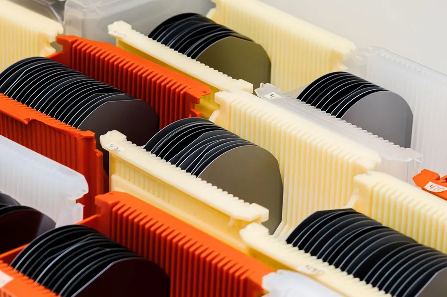
Shop NowSilicon wafer processing plays a critical role in semiconductor production, the building blocks of nearly every modern electronic device. As the electronics industry continues to advance, silicon wafer processing must evolve to meet the increasing demand for faster, smaller, and more efficient devices. Recent innovations in this field are helping improve the performance, reliability, and cost-effectiveness of silicon wafers, paving the way for the next generation of electronic products.
One of the most impactful advancements in silicon wafer processing has been the development of more precise and efficient lithography techniques. Lithography, a process used to etch patterns onto the wafer's surface, is critical in creating the intricate circuits found in modern microelectronics. Recent innovations in extreme ultraviolet (EUV) lithography have enabled manufacturers to etch smaller, more complex patterns, enabling the creation of faster, more powerful semiconductors.
Another major innovation is the improvement of chemical vapor deposition (CVD) techniques used to deposit thin films on silicon wafers. These films play an essential role in the performance of semiconductor devices. Enhanced CVD processes now allow the deposition of higher-quality films with fewer defects, thereby improving device performance.
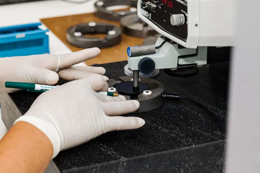
Additionally, advances in wafer polishing and chemical-mechanical planarization (CMP) have helped improve the flatness and uniformity of wafers. By ensuring the surface of each wafer is smoother and more consistent, these innovations improve yields and reduce defects in semiconductor manufacturing.
As demand for more powerful and efficient electronics continues to rise, silicon wafer processing will remain a key focus of innovation. Manufacturers are constantly exploring new materials and techniques to improve the processing of silicon wafers. For example, the use of new materials, such as gallium arsenide (GaAs), in combination with silicon, is being explored to push the boundaries of what’s possible in semiconductor technology.
The latest innovations in silicon wafer processing are enabling the development of more efficient, reliable, and high-performing electronic devices. At Wafer World, we are committed to providing the highest-quality wafers for your semiconductor needs. Whether you’re working on next-generation devices or looking to improve your existing production processes, our advanced wafers meet the highest industry standards. Contact us today to learn how we can support your wafer needs and drive your success in the electronics industry.


