Technology continues to push semiconductor manufacturing toward greater precision, cleaner surfaces, and more reliable performance. As device designs become smaller and more complex, silicon wafer processing plays an increasingly important role in supporting quality, consistency, and long-term functionality across advanced applications.
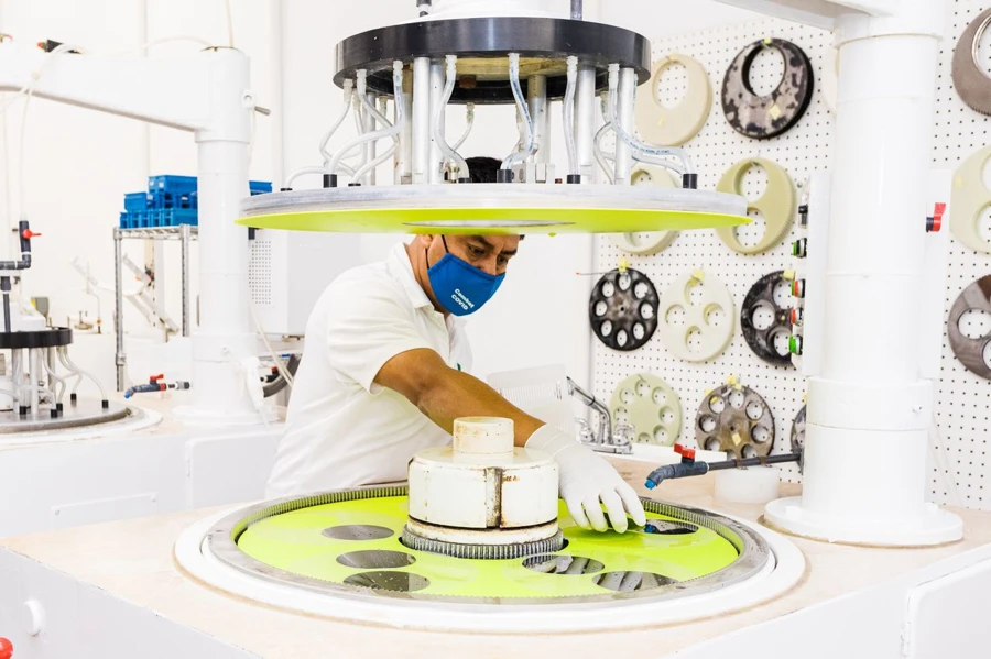
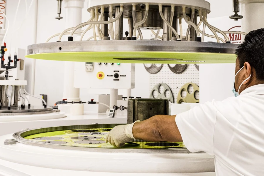
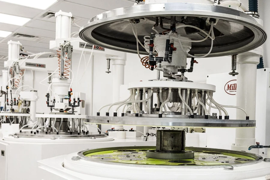
Clean wafer surfaces are essential for reliable manufacturing. Modern cleaning methods help remove particles, residues, and other contaminants before wafers move to subsequent production steps. Even a small surface defect can affect performance, so manufacturers rely on controlled cleaning systems, improved chemical processes, and advanced inspection tools to help maintain wafer integrity.
A smooth, consistent surface supports better layering, bonding, and patterning. This is especially important for applications that require tight tolerances and dependable electrical behavior.
Automation has helped make wafer production more consistent. With advanced sensors and monitoring systems, manufacturers can track conditions in real time and adjust key variables with greater accuracy. This reduces human error and helps support repeatable results across production batches.
Important improvements include:
Inspection tools continue to improve as wafer requirements become more demanding. High-resolution imaging, metrology systems, and automated testing help identify defects earlier in the process. Early detection supports higher yields, reduces material waste, and provides manufacturers with useful data for future process improvements.
Data analysis allows teams to identify patterns, monitor process drift, and make informed adjustments. This helps create a more stable manufacturing environment while supporting long-term quality goals.
Innovations in wafer processing are not only about speed. They also aim to improve reliability, reduce defects, and help manufacturers meet evolving performance standards. Better tools and tighter controls can support stronger yields while helping wafers perform consistently in demanding applications.
Choosing the right wafer starts with understanding the process, quality expectations, and application requirements behind it. For guidance on specifications, material considerations, or project planning, contact us today to schedule a consultation or call the Wafer World team to discuss silicon wafer processing options for your next application.


