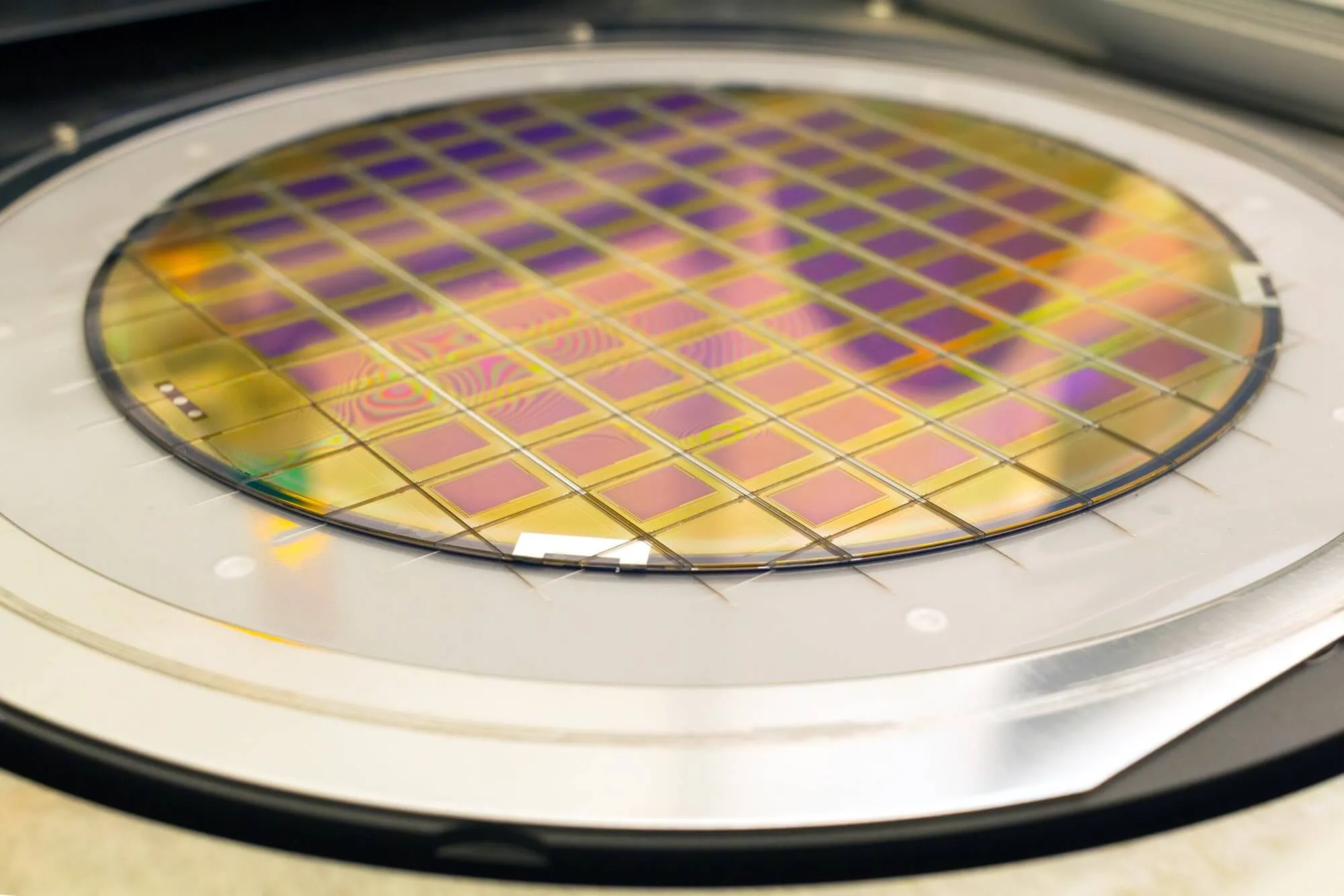
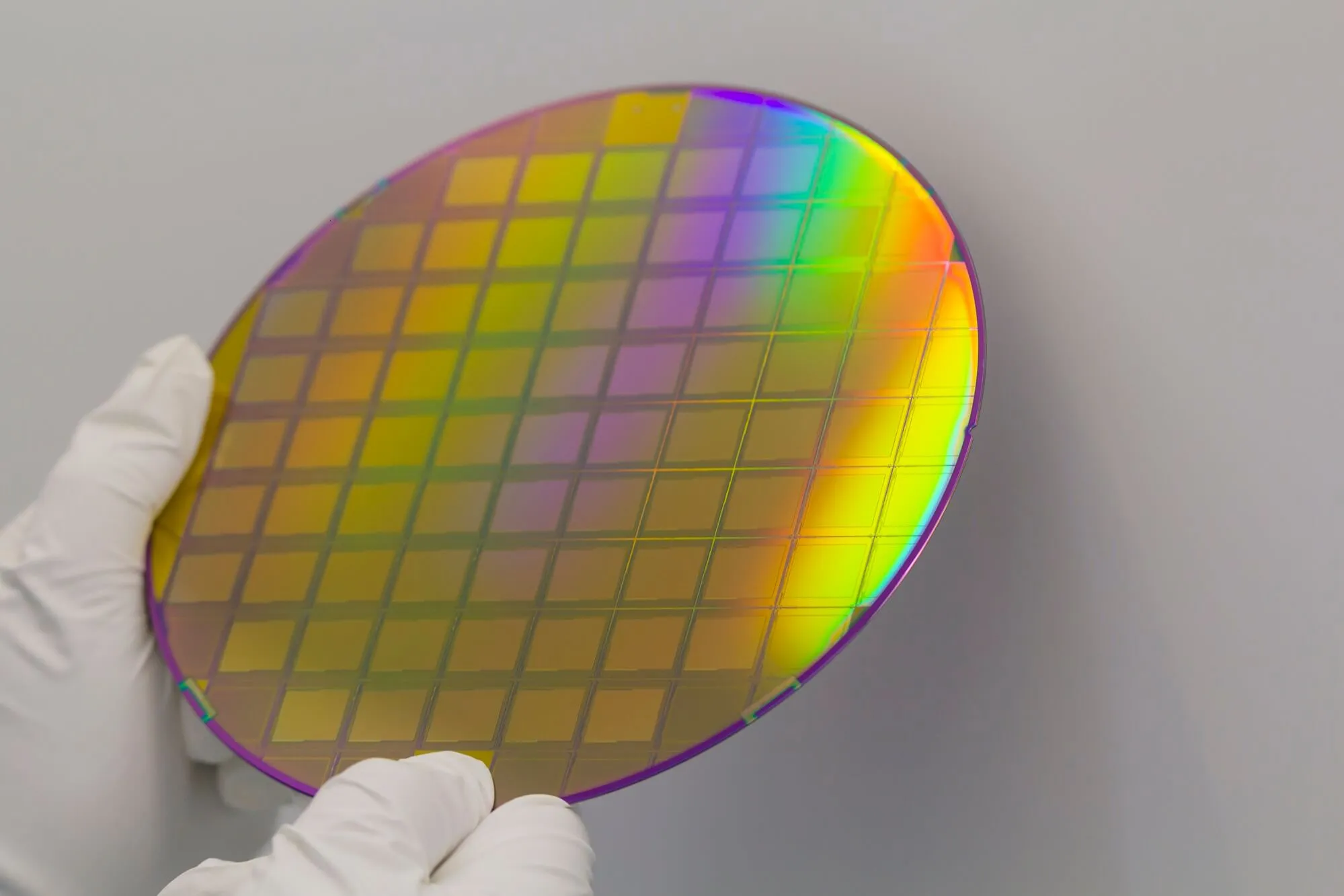
In the world of semiconductor materials, indium phosphide (InP) has emerged as a remarkable contender due to its unique properties and versatile applications. InP wafers have gained significant attention in the semiconductor industry for their excellent electronic, optical, and mechanical characteristics. In this blog post, we will delve into the fascinating properties and characteristics of InP wafers and explore the various applications that make them an integral part of advanced technology.
One of the most distinctive features of InP wafers is their narrow direct bandgap of approximately 1.35 eV at room temperature. This bandgap allows InP to absorb and emit light efficiently in the infrared (IR) region. This property makes InP wafers ideal for applications in optoelectronic devices, such as photodetectors, lasers, and light-emitting diodes (LEDs).
InP wafers possess impressive electron mobility, which is a crucial parameter for high-speed electronic devices. With electron mobilities exceeding 4000 cm²/V·s, InP outperforms many other semiconductor materials like silicon and gallium arsenide. This high mobility is particularly beneficial for the development of high-frequency transistors and integrated circuits.
InP wafers exhibit excellent thermal stability and can withstand high temperatures without significant degradation. This property makes them suitable for use in high-power electronic devices where heat dissipation is a concern. InP wafers are also highly resistant to thermal stress, ensuring the reliability of devices in demanding environments.
InP wafers exhibit low dispersion characteristics, particularly in the infrared spectrum. Dispersion refers to the phenomenon where different wavelengths of light travel at different speeds through a material, leading to the spreading of optical signals.
InP's low dispersion property is particularly valuable in optical communications, where it helps maintain the integrity of data transmission by minimizing signal distortion and ensuring that different wavelengths of light remain synchronized. This makes InP wafers an excellent choice for the development of optical waveguides and components used in high-capacity optical communication systems and fiber optic networks.
InP wafers have low levels of intrinsic noise, making them ideal for applications in low-noise amplifiers and high-frequency communication systems. Their low noise performance is a crucial factor in enhancing the signal-to-noise ratio in electronic circuits, leading to improved overall system performance.
InP wafers have a high breakdown voltage, which means they can handle higher electric fields without breaking down. This property is advantageous in power electronics and high-voltage applications, where the ability to withstand large voltages is essential.
InP wafers are known for their ability to operate across a wide temperature range, from cryogenic temperatures to elevated temperatures exceeding 100°C. This characteristic makes InP suitable for applications in extreme environments, such as aerospace and military systems.
InP wafers can be integrated with other semiconductor materials like gallium arsenide (GaAs) and indium gallium arsenide (InGaAs) to create heterostructures. These heterostructures enable the design and fabrication of advanced devices with tailored properties, such as high electron mobility transistors (HEMTs) and quantum well lasers.
InP wafers have a wide range of applications across various fields due to their unique properties. Let's explore some more applications of InP wafers:
InP wafers are widely used in the manufacture of optoelectronic devices, including high-speed photodetectors, lasers, and LEDs, for applications in telecommunications, optical fiber networks, and spectroscopy.
InP wafers find applications in high-frequency and high-speed electronic devices, such as HEMTs and integrated circuits, for use in wireless communication systems and radar technology.
InP solar cells offer high efficiency for converting sunlight into electricity, making them suitable for space applications and high-efficiency terrestrial photovoltaic systems.
InP wafers are radiation-resistant, making them suitable for use in space exploration and nuclear environments where radiation tolerance is critical.
InP wafers are used to create components for fiber-optic communication systems. Their ability to efficiently emit and detect light in the infrared region makes them ideal for the production of high-performance optical modulators and receivers in fiber-optic networks.
InP wafers are used to develop terahertz (THz) emitters and detectors. THz radiation has applications in imaging, spectroscopy, and security screening, and InP-based devices play a crucial role in advancing THz technology.
InP wafers are used to create quantum dots, which are nanoscale semiconductor particles with unique electronic properties. Quantum dots made from InP have applications in quantum computing, quantum cryptography, and advanced displays with improved color purity.
InP solar cells are highly efficient and radiation-resistant, making them ideal for use in space missions where energy generation is critical. They are employed in solar panels on satellites and spacecraft.
InP-based detectors are used in medical imaging devices such as positron emission tomography (PET) scanners. These detectors can provide high-resolution images for accurate diagnosis and treatment planning.
InP wafers are utilized in various types of sensors and detectors, including gas sensors and chemical sensors. Their sensitivity and reliability make them valuable in environmental monitoring and industrial applications.
InP wafers are used in defense and security applications, including radar systems, night vision technology, and secure communication systems. Their high-frequency capabilities and radiation resistance are advantageous in these fields.
InP wafers are employed in quantum optics experiments and quantum information processing. Researchers use them to create quantum entanglement and quantum key distribution systems for secure communication.
InP wafers are the foundation for photonic integrated circuits (PICs), which can combine various optical components on a single chip. PICs find applications in data centers, telecommunications, and optical signal processing.
InP-based devices are utilized in biomedical applications, such as non-invasive glucose monitoring, where the high sensitivity of InP detectors is advantageous for accurate measurements.
InP wafers have become indispensable in the semiconductor industry due to their exceptional properties and characteristics. Their wide-ranging applications in optoelectronics, high-frequency electronics, and extreme environments highlight their versatility and significance in advancing technology. As research and development continue, InP wafers are poised to play an even more pivotal role in shaping the future of electronics and photonics.
Wafer World has the widest variety of wafers in the market! Call now to know more!


