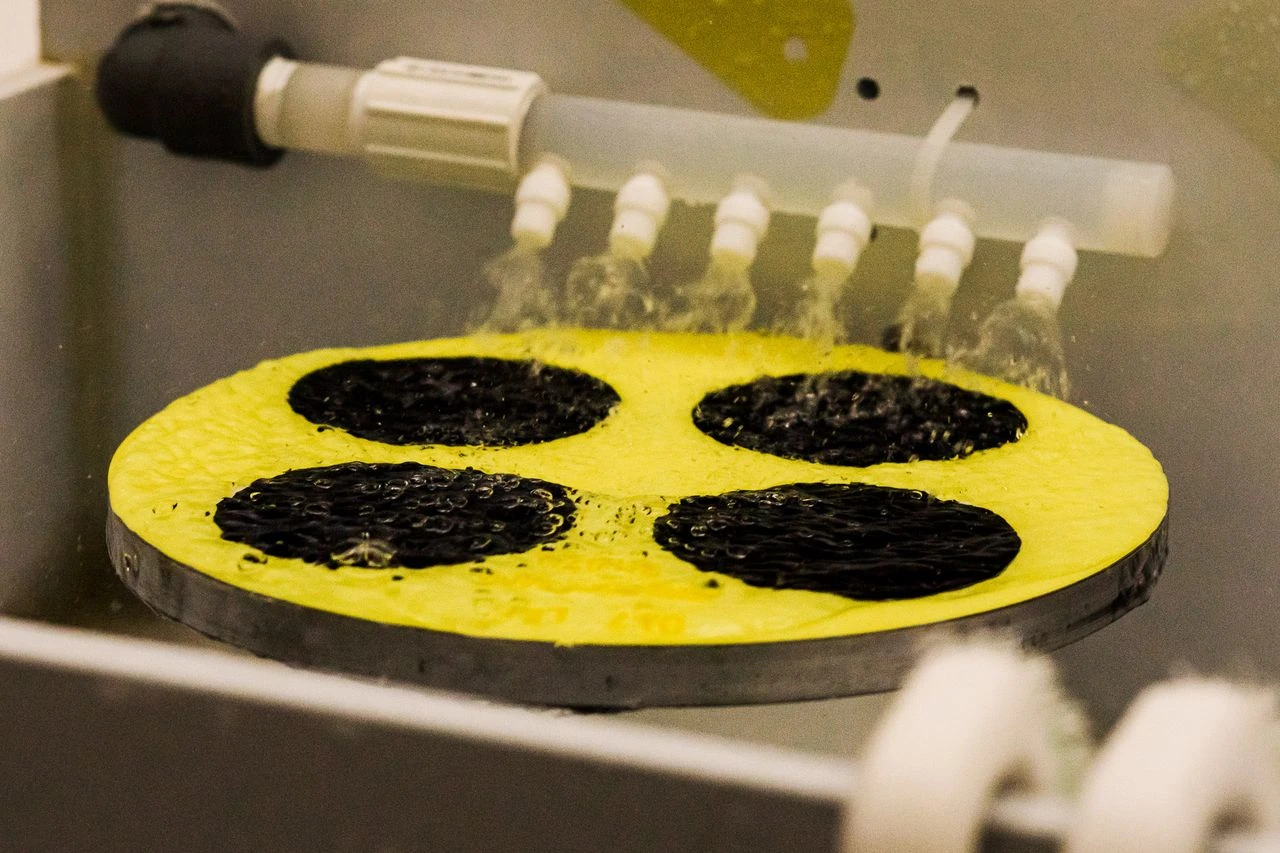
Selecting the right wafer material is one of the most important steps in semiconductor manufacturing, research and development, photovoltaic systems, and microelectronic production. Teams that buy silicon wafer materials for technical applications often focus on pricing first, but long-term performance usually depends on material quality, consistency, and specification accuracy. Even a small variation in thickness, resistivity, or crystal orientation can affect production outcomes, device reliability, and fabrication efficiency.
Silicon wafers are used across a wide range of industries due to their electrical properties, thermal stability, and compatibility with modern fabrication techniques. However, not every wafer is designed for the same environment or performance level. Some applications require ultra-flat polished wafers for integrated circuits, while others may prioritize reclaimed wafers for testing or process monitoring. Understanding the differences between wafer grades, substrate quality, and manufacturing standards can help buyers avoid unnecessary waste and production setbacks.
Silicon wafers are commonly categorized into different grades based on intended use, surface quality, and manufacturing precision. Prime-grade wafers are often selected for advanced semiconductor manufacturing because they meet stringent standards for flatness, particle control, and surface defect levels. These wafers are generally used in high-performance applications where consistency is critical.
Test grade wafers are another common option. They are frequently used for equipment calibration, training, process monitoring, and early-stage research. While they may contain minor imperfections, they can still provide dependable results for non-production environments.
Reclaim wafers offer an economical alternative for facilities that need cost-efficient materials for monitoring or experimentation. These wafers are processed to remove prior film layers and contaminants before reuse. For many organizations, reclaim wafers help reduce material costs while supporting sustainability goals.
Epitaxial wafers feature a thin deposited layer that improves electrical performance and supports advanced semiconductor structures. These wafers are often used in power devices, sensors, and specialized integrated circuits that require controlled electrical behavior.
Crystal orientation affects how wafers behave during fabrication and device production. Common orientations include <100>, <110>, and <111>. Each orientation supports different etching behaviors, mechanical characteristics, and electrical properties.
The <100> orientation is frequently used in semiconductor manufacturing because it provides reliable oxidation characteristics and supports many integrated circuit processes. The <111> orientation may be selected for applications requiring specific mechanical or etching properties.
Resistivity is another important factor when evaluating wafer materials. It measures how strongly silicon opposes the flow of electrical current. Depending on the application, buyers may need wafers with low, medium, or high resistivity ranges.
Doping type also plays a major role. P-type wafers contain dopants that create positive charge carriers, while N-type wafers create negative charge carriers. The required conductivity type depends on the intended electrical application and manufacturing process.
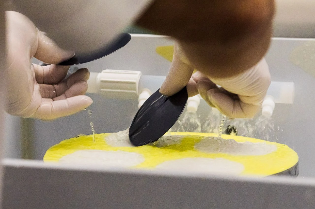
Surface quality directly influences lithography, deposition, and etching performance. Polished wafers are designed to provide smooth surfaces that support precision manufacturing. Single-side polished wafers are commonly used when only one active side is required, while double-side polished wafers offer uniformity on both surfaces.
Flatness is especially important in advanced fabrication environments. Variations in total thickness or bow can create alignment issues during photolithography and wafer handling. Manufacturers often evaluate total thickness variation, warp, and bow to confirm process compatibility.
Particle contamination can also affect wafer performance. Even microscopic contaminants may interfere with device yields or introduce defects into production lines. Clean handling procedures and controlled packaging are often necessary to maintain wafer integrity during shipping and storage.
Wafer dimensions must align with the requirements of the manufacturing equipment and the application demands. Common wafer diameters include 2-inch, 4-inch, 6-inch, 8-inch, and 12-inch formats. Larger wafers generally support higher production volumes because more devices can be fabricated on a single substrate.
Thickness consistency is another major consideration. Uneven wafers may create processing challenges during polishing, coating, or etching. Tight dimensional tolerances help manufacturers maintain stable production conditions and reduce variability.
Edge profiles also influence wafer handling and durability. Properly engineered edge designs help reduce the risk of chipping or cracking during transportation and processing. Since wafers are extremely delicate, even minor edge damage can compromise usability.
Manufacturing facilities should also confirm notch or flat orientation specifications before placing orders. These features help identify crystal orientation and ensure compatibility with automated handling systems.
High-purity silicon is essential for maintaining stable electrical behavior and reducing defects during fabrication. Impurities can alter conductivity, affect thermal performance, or interfere with layer deposition.
Manufacturers often inspect wafers for particles, scratches, haze, pits, and crystal imperfections before shipment. Inspection procedures may involve optical scanning, metrology systems, or automated surface analysis.
Defect density becomes especially important in advanced semiconductor applications where extremely small circuit structures are involved. Even minimal contamination or surface irregularities can affect device reliability and production yields.
Oxygen and carbon concentrations are also monitored in many wafer applications. These elements may influence mechanical strength, thermal characteristics, and internal crystal quality. Understanding these specifications helps buyers select materials suited to their fabrication environment.

Reliable sourcing is about more than immediate availability. Manufacturers and research facilities often depend on consistent wafer specifications across multiple production cycles. Variations between batches may create calibration issues, yield fluctuations, or unexpected process adjustments.
Working with experienced suppliers can help organizations maintain specification consistency and traceability. Many facilities request detailed documentation regarding wafer origin, polishing methods, resistivity ranges, and inspection standards before approving materials for production.
Lead times and inventory planning also matter in industries with strict production schedules. Delays in wafer availability can interrupt manufacturing timelines and increase operational costs. Establishing dependable procurement strategies may reduce these risks.
Environmental handling practices should also be considered. Proper packaging, contamination control, and transportation procedures help preserve wafer quality from shipment through final use.
Choosing wafer materials without reviewing technical specifications can create costly production challenges later. Every application has unique performance requirements, whether the focus is semiconductor fabrication, MEMS devices, photovoltaics, or university research.
A detailed evaluation process helps buyers confirm compatibility with manufacturing equipment, thermal requirements, electrical performance targets, and process tolerances. Reviewing crystal orientation, resistivity, surface finish, flatness, and defect density together provides a more complete understanding of wafer suitability.
Organizations that prioritize technical review often experience fewer process interruptions, more stable yields, and improved long-term efficiency. Instead of relying on generalized material descriptions, it is more effective to compare detailed wafer specifications directly against operational requirements.
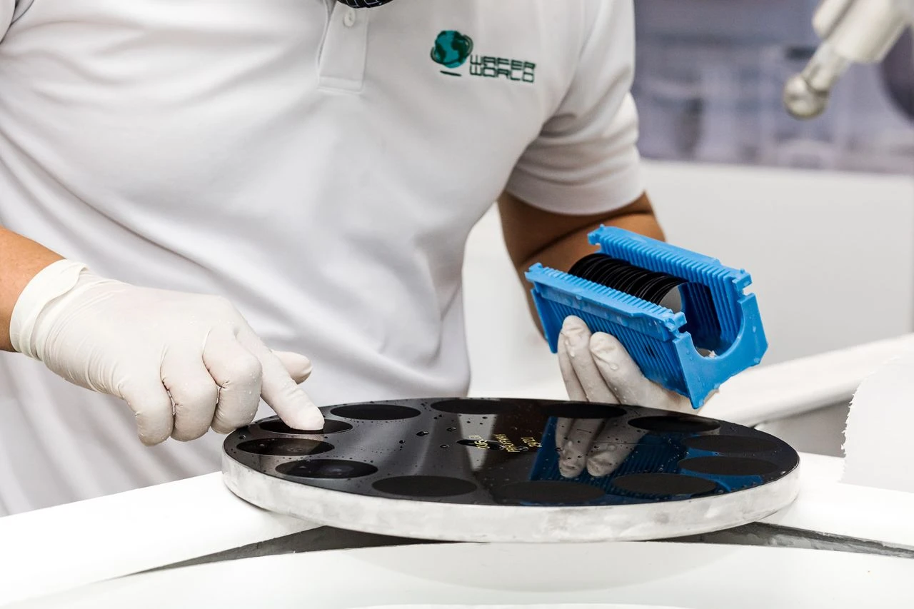
Carefully reviewing wafer grades, dimensional tolerances, electrical characteristics, and surface quality can help manufacturers and research teams make informed procurement decisions. If you are preparing to buy silicon wafer products for semiconductor, testing, or research applications, taking time to evaluate material specifications now may help reduce future production risks and improve long-term consistency. Wafer World supports customers with silicon wafer solutions tailored to a wide range of technical and industrial requirements. Contact us today to discuss your project specifications or schedule a consultation with our team.




