As semiconductor devices continue to scale down, the choice of wafer substrate becomes just as important as the circuit design itself. Many engineers and procurement teams ask the same question: When do thin silicon wafers need epitaxial layers—and when is standard silicon enough?
Epitaxial (epi) wafers are not a universal requirement, but when needed, they address very specific electrical, structural, and yield-related challenges. Understanding what epi wafers are, how they’re made, and—most importantly—when using them makes sense from both a technical and economic perspective is crucial for fabs and manufacturers.
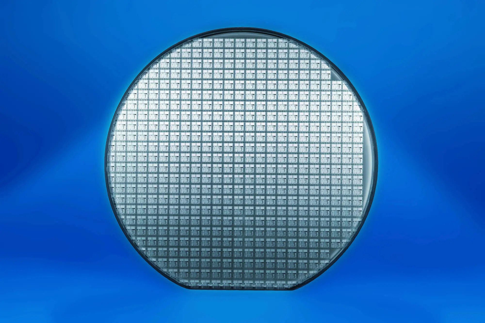
Thin silicon wafers are substrates that have been thinned below conventional thicknesses to meet performance, packaging, or integration requirements. They are widely used in advanced logic, memory, power devices, and 3D integration schemes.
However, thinning a wafer amplifies several inherent material limitations. As wafers become thinner, bulk defects, dopant variations, and substrate noise have a greater impact on device behavior. This is where epitaxial layers often become essential—not optional.
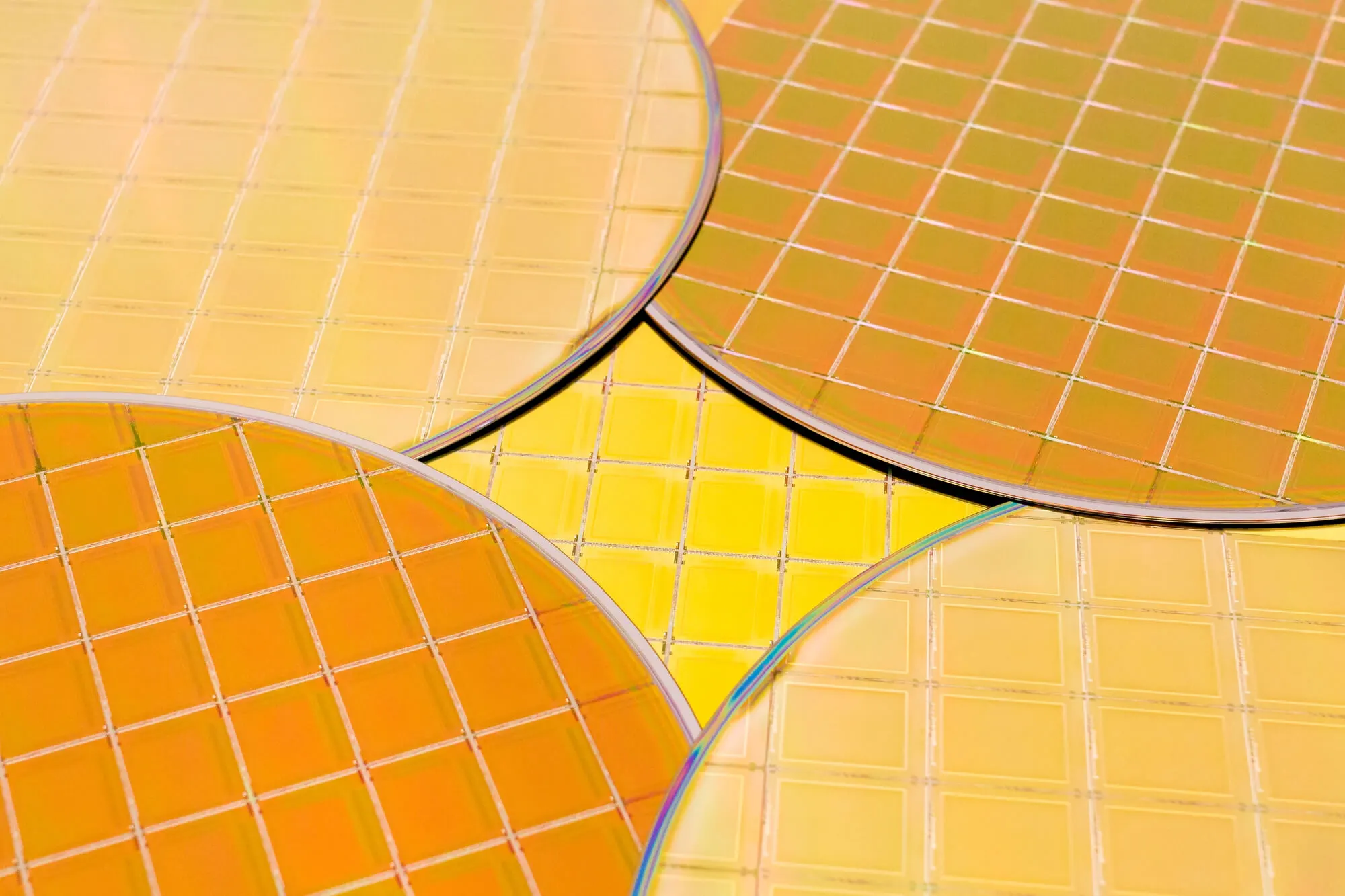
Epitaxy refers to the growth of a thin, single-crystal layer of silicon on top of a silicon wafer. The epitaxial layer follows the crystal structure of the underlying substrate but can be engineered with precisely controlled thickness, doping concentration, and resistivity.
Unlike bulk silicon, which inherits its properties from crystal growth, epitaxial silicon is custom-built for device requirements. This makes epi wafers especially valuable when thin silicon wafers are pushed to their limits in terms of electrical or mechanical properties.
Not every application requires an epi wafer. However, epi becomes critical when thin silicon wafers are used in scenarios where electrical precision, defect isolation, or device uniformity cannot be compromised.
Epitaxial wafers are typically required when devices demand tight control over dopant profiles, reduced leakage currents, or isolation from bulk substrate defects. This includes advanced CMOS logic, RF devices, power semiconductors, and many analog applications.
Thin wafers used in high-voltage or high-frequency environments also benefit from epitaxial layers, which allow engineers to decouple surface device behavior from the bulk substrate. In short, when performance margins shrink, epi wafers provide the process control needed to maintain yield and reliability.
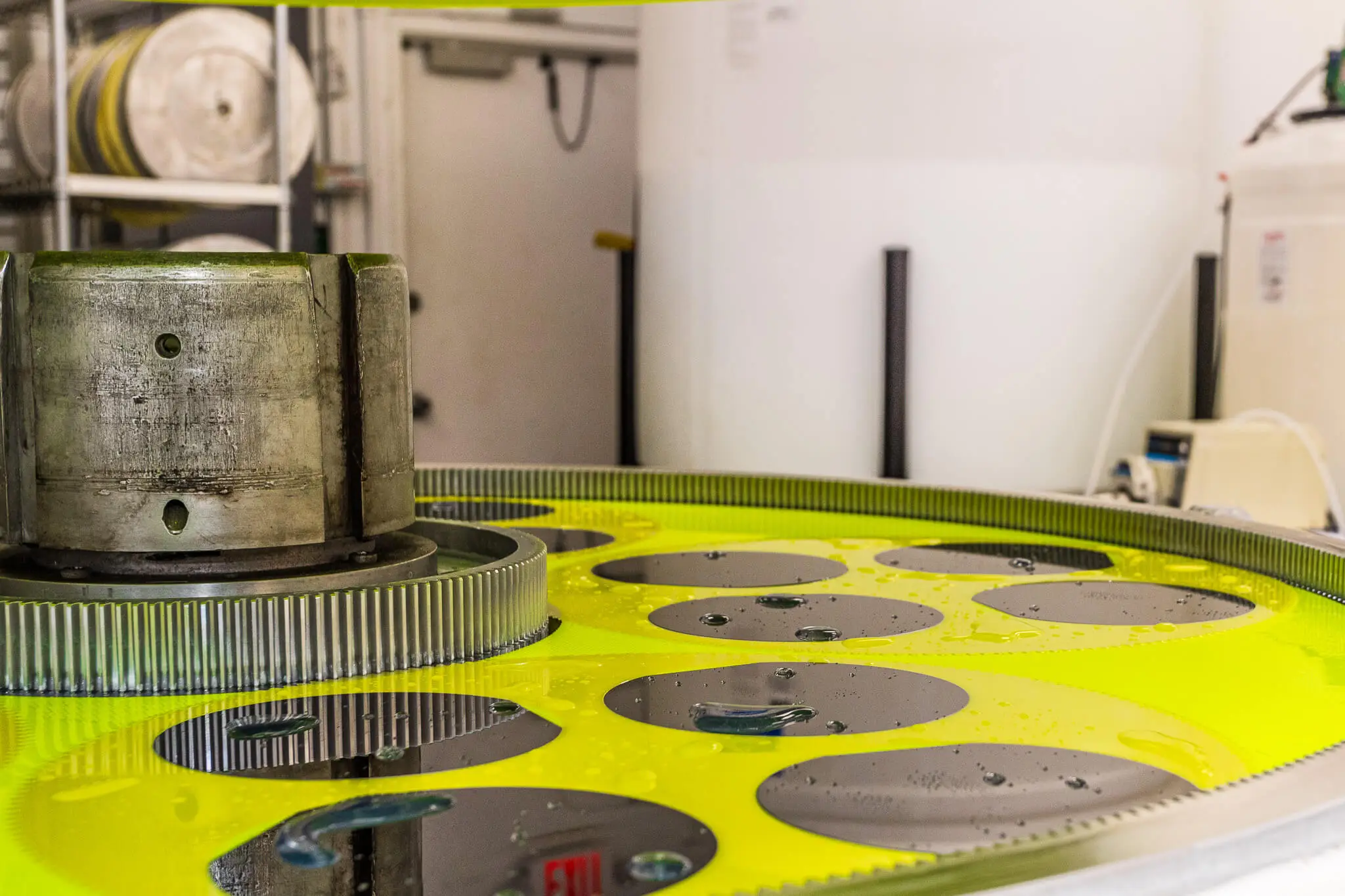
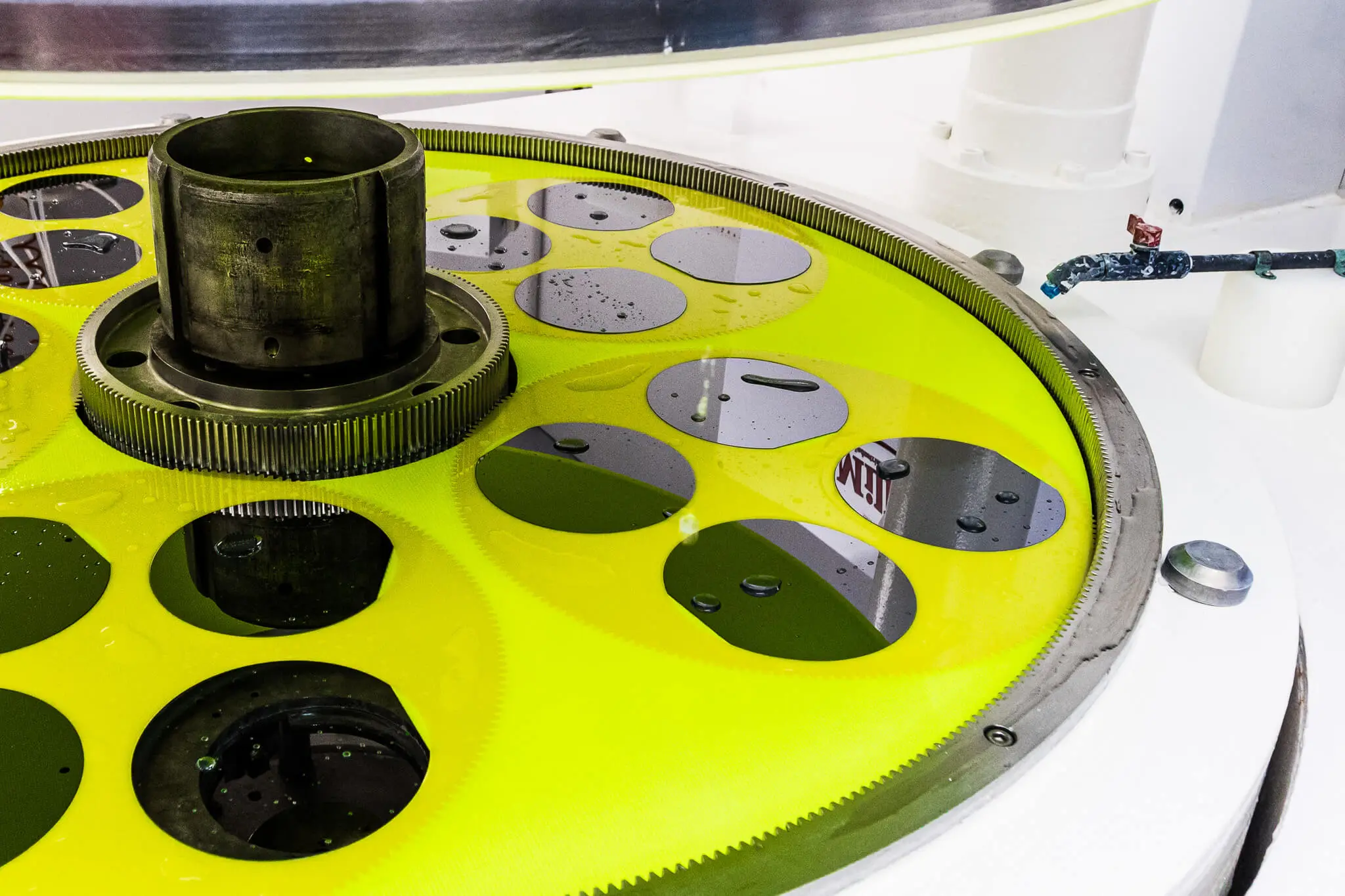
The manufacturing process for epitaxial wafers begins with a carefully prepared silicon substrate, often a polished or double-sided polished wafer. Surface cleanliness and crystal quality are critical, as any defects present on the substrate can propagate into the epitaxial layer.
Epitaxial growth is typically performed using Chemical Vapor Deposition (CVD). During this process, silicon-containing gases are introduced into a high-temperature reactor, where they decompose and deposit silicon atoms onto the wafer surface in a precise, crystal-aligned manner. Dopant gases can be added simultaneously, allowing precise control of electrical properties.
The result is a thin, highly uniform silicon layer that can range in thickness from fractions of a micron to several microns, depending on the application. For thin silicon wafers, this engineered layer often becomes the active device region, while the underlying substrate provides mechanical support.
The most important difference between epitaxial and standard silicon wafers lies in control. Standard wafers rely entirely on the properties of the bulk crystal, which are suitable for many applications but inherently limited in flexibility.
Epitaxial wafers allow manufacturers to define electrical behavior at the surface independently of the substrate. This results in lower defect density in the active region, more consistent resistivity, and enhanced isolation. For thin wafers, these advantages become even more pronounced, as there is less bulk material to absorb variability.
That said, epitaxial wafers introduce additional manufacturing complexity and cost. The key is understanding whether the performance gains justify that investment, which depends entirely on the device being built.
Epi wafers offer unique benefits, such as:
Yield losses in semiconductor manufacturing are often traced back to substrate-related issues. Standard wafers may contain bulk defects that are acceptable for some applications but problematic for others—especially when wafers are thinned.
Epitaxial layers effectively “reset” the surface quality, creating a pristine starting point for device fabrication. This significantly reduces the impact of substrate defects on the active region, thereby improving overall yield, particularly in advanced nodes or sensitive analog designs.
For fabs working with thin silicon wafers, this yield improvement can offset the higher cost of epitaxial processing.
Epitaxial wafers are widely used in advanced CMOS logic, where tight electrical control is essential. They are also common in RF front-end modules, power management ICs, and automotive electronics, where reliability and consistency are non-negotiable.
Thin wafers used in 3D integration, wafer-level packaging, or backside processing frequently rely on epi layers to maintain device integrity as mechanical thickness is reduced. In these cases, epitaxy acts as an enabler, allowing aggressive thinning without sacrificing performance.
If your application can tolerate higher defect densities, broader resistivity ranges, and bulk substrate influences, standard silicon wafers may be sufficient. However, if you are working with thin wafers in performance-critical environments, epitaxial wafers are often the safer and more scalable choice.
Device requirements, not habit, should drive the decision. Evaluating electrical performance targets, yield sensitivity, and long-term reliability will quickly clarify whether epitaxy is necessary.
Epitaxial wafers are not just a premium option—they are a problem-solving tool. For thin silicon wafers used in advanced semiconductor devices, epitaxy provides the control, consistency, and performance needed to stay competitive as designs continue to scale.
Finding the right thin silicon wafers is also crucial for simplifying fabrication, improving yield, and unlocking higher-value applications. Whether you need standard substrates, custom epitaxial layers, or thin wafer solutions optimized for your process, Wafer World can help. Contact our team to discuss your application and find the right wafer solution for your device roadmap!


