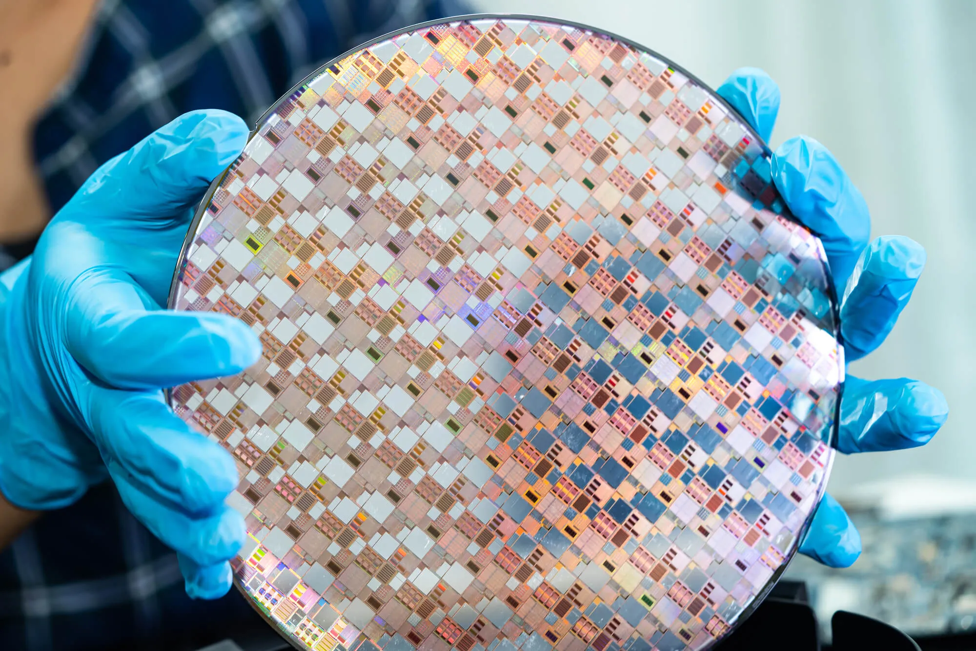
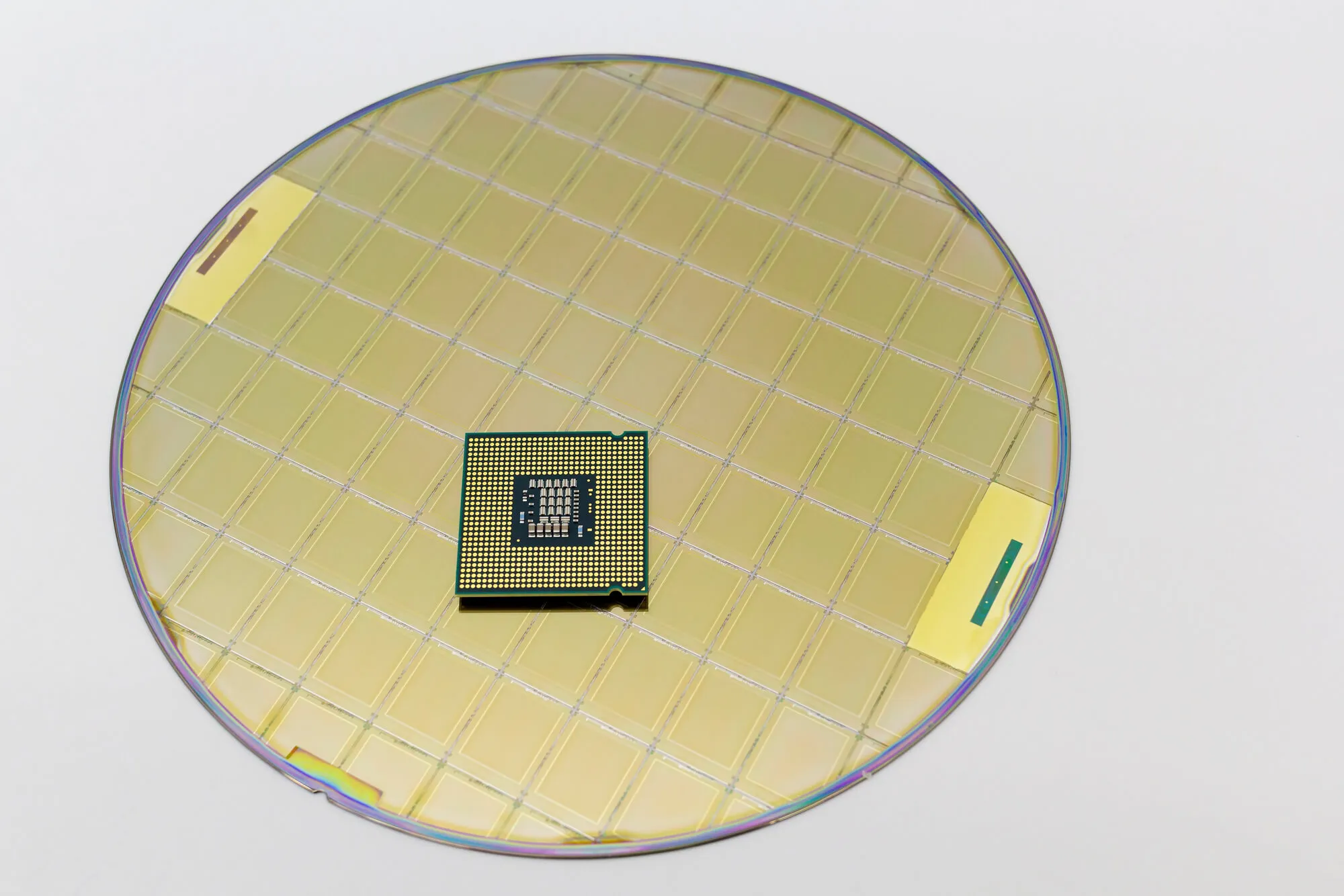
Silicon wafers are the backbone of modern electronics and semiconductors, and the quality of these wafers is critical to ensuring the performance and reliability of these devices. One key aspect of ensuring high-quality silicon wafers is the process of defect detection, which involves identifying and eliminating defects in the manufacturing process. In this article, we'll explore the defect detection process and the importance of quality control in silicon wafer manufacturing.
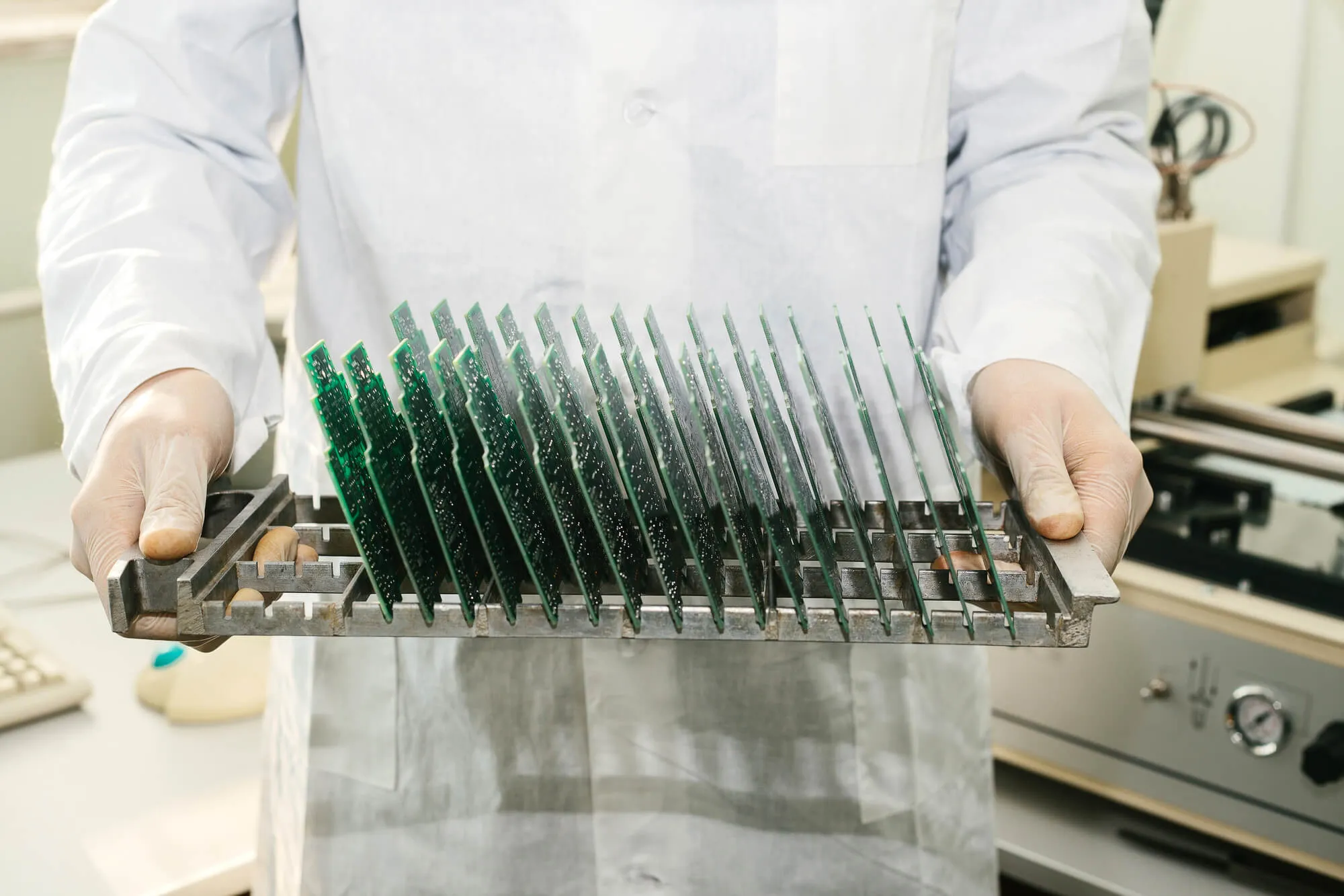
The defect detection process is crucial to silicon wafer manufacturing. It involves several steps, including inspection and metrology techniques, to identify and measure defects in the wafers. The goal is to eliminate defects that can affect the final product's performance, such as cracks, contamination, and variations in thickness.
Manufacturers use various technologies to detect defects, including optical inspection, X-ray imaging, and electron microscopy. These techniques detect even the smallest defects, ensuring that only high-quality wafers are used in producing electronics and semiconductors.
Maintaining high levels of precision and consistency is essential for producing high-quality silicon wafers. Quality control measures are implemented to monitor and improve the manufacturing process, ensuring that defects are eliminated, and consistent quality is maintained.
Statistical process control (SPC) is a common method used for quality control in silicon wafer manufacturing. SPC involves monitoring and analyzing data from the manufacturing process to identify patterns and trends, allowing for the early detection of potential issues. This approach helps ensure that the manufacturing process operates within acceptable parameters and that deviations from the norm are quickly identified and addressed.
Emerging technologies, such as machine learning and artificial intelligence, are being developed to improve defect detection in silicon wafer manufacturing further. These technologies can improve the speed and accuracy of defect detection, reducing the risk of defects slipping through the manufacturing process undetected.
However, implementing these advanced techniques comes with challenges, including the need for high-quality data and the ethical and social considerations related to automation in the manufacturing process.
The importance of defect detection and quality control in silicon wafer manufacturing will only grow as the demand for high-quality electronics and semiconductors increases. As such, manufacturers will likely continue investing in new technologies and techniques to improve the manufacturing process.
Automation and artificial intelligence are likely to become increasingly prevalent, offering the potential for increased efficiency and cost savings. However, ensuring these technologies are implemented ethically and responsibly will be important, with proper consideration given to the potential impact on the workforce and society.
At Wafer World, our team can provide you with silicon and semiconductor wafer services. Give us a call today to learn more about the services we offer!


