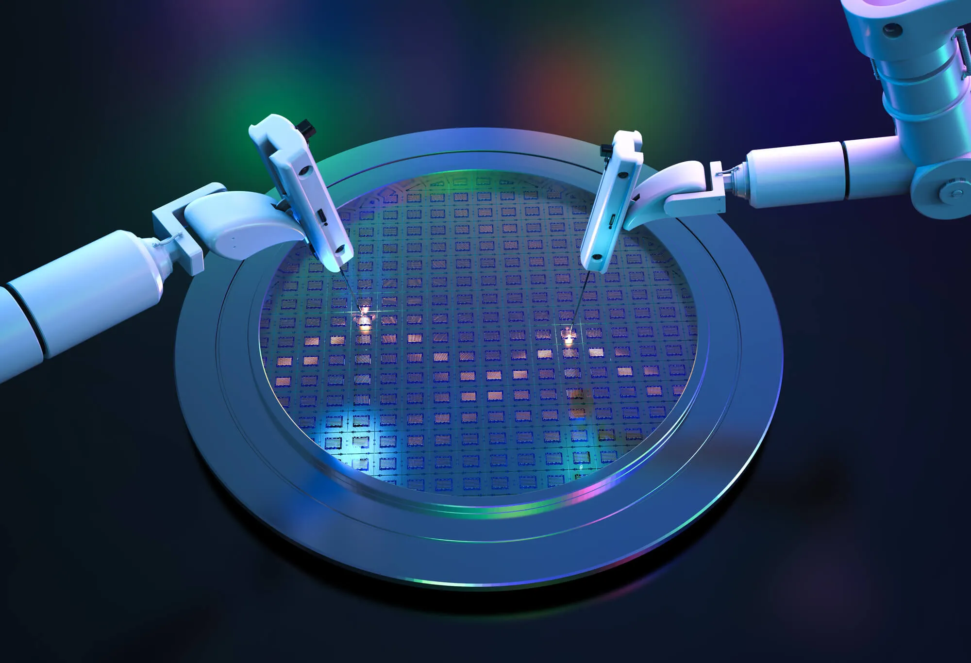
Silicon wafer processing is a meticulous procedure. Both methods used in creating silicon wafers from ingots are fully automated to minimize human error. However, there is still a remote chance that the finished product may have defects that can hamper the wafer from doing its job correctly.
Chips are also prone to manufacturing flaws, more so than wafers. There are numerous components within a single motherboard or memory. These can only optimally function when they are arranged in a specific manner. Imperfections could also result in reduced performance and damage to the equipment using the chip.

Quality control ensures that the final product is free of defects. The QA process is the vital barrier between low-quality semiconductors and the consumer market.
For computer chips, minute flaws in their construction can cause current leakage and voltage fluctuations. These two events can significantly damage the computer and its peripherals that rely on electric current to properly work.
Aside from the physical damage, cybersecurity researchers in 2019 reported that defects in older chips left computers built from 2017 onwards vulnerable to seven threats. Most of the defective chips discovered by the research were manufactured by Intel. At the same time, AMD processors faced weakness in only one identified risk.
On the other hand, manufacturing defects on wafers can either make them inefficient in function or totally useless. Three defects in wafers could be spotted during an optical inspection, namely:
Despite being minor, these faults are difficult to spot visually. They can degrade their ability to fulfill their purposes. For instance, grinding flaws in wafers used in car electronics can become unreliable at high temperatures. Worse, these imperfections can cause the chips to fail.
This term covers flaws like unequal thickness, dislocation, Frenkel imperfections, dislocation loops, etc. These silicon wafer processing deficiencies make the wafer unable to perform as intended. However, it can still be utilized for testing purposes.
Critical defects include cracks and chipping in the wafer body, dust contamination, and peeled metal. The wafer is automatically discarded when QA personnel find any of these defects.
Ocular inspection for defects in both chips and wafers becomes even more challenging as chip manufacturers continue to follow Moore’s Law.

Moore’s Law refers to how computers become more powerful with every generation by simply doubling the number of transistors in the chipset. The law is the empirical observation of Gordon Moore, a co-founder of Intel. While it was never a rule of thumb in chip-making, the industry stuck to this standard in innovating products throughout the decades.
These companies cram twice the number of transistors from previous models into the next iteration’s circuit board to keep up with Moore’s Law. After decades of this practice, the average consumer can now build significantly powerful rigs with billions of transistors on a processor smaller than one’s palm.
While computers progressively surpass their predecessors’ performance, quality control becomes more challenging. This is due to the sheer number of transistors to inspect in a chip and the size of each node. Imaging techniques like Terahertz imaging may help significantly.
Terahertz imaging is a non-invasive, non-destructive optical technology used in multiple fields. The technique involves light waves with frequencies between 100 Gigahertz and 10 Terahertz and wavelengths between 3 millimeters and 30 micrometers.
Astronomers primarily utilized the tech to study celestial bodies that are not visible in the night sky due to their distance from our solar system. In recent years, however, terahertz imaging found applications in various industries, including semiconductor manufacturing and quality control.
In THz imaging, a lightwave emitter transmits pulsed lightwaves from various directions to the specimen the machine needs to scan. These pulses either pass through the sample or get reflected towards a detector. Afterward, the sensor analyzes the captures from multiple pulses and generates a three-dimensional image.
Terahertz imaging is ideal for visually examining semiconductors because it does not further ionize the metal. Silicon wafers are already ionized to manipulate their conductive properties before being submitted for quality control. Introducing additional ions will upset the electron balance already set during the manufacturing process.
Second, light waves in the terahertz spectrum can pass through any surface, whether conductive or non-conductive. THz scanning can see through materials such as fabric, wood, paper, plastic, and cardboard better than microwave signals. It can also scan objects in real-time.
Lastly, THz imaging outputs pictures with high-contrast and high spatial resolution, which results in excellent detail. It’s easier for QA personnel to spot defects in every wafer or chip they check the quality of. The images’ accuracy minimizes the odds of defective products making it out of the manufacturing facility.
Terahertz imaging has numerous potential applications in the medical industry. One field that it could be instrumental in is cancer research. The non-invasive imaging that THz radiation renders could allow oncologists to detect cases without a biopsy. In other words, THz scanning can potentially spot cancer early before it spreads throughout the body.
THz technology is also at home in the defense and security niche. The light waves’ penetrating ability can discover hazardous materials and weapons hidden in baggage and within the persons themselves. In fact, this industry has seen significant developments in its application of Terahertz technology.
Finally, terahertz technology could also be used in art studies and preservation. Its scanning capabilities can reveal hidden murals in old buildings worldwide without tearing down the current exterior. This method can help art aficionados and archaeologists save money and time on their work.

Our stringent quality control processes ensure that our wafers are free from the three defects. What you get are perfectly shaped products that are highly efficient in their performance. Contact us now for a quote.


