Gallium Arsenide is a faster and more efficient substrate for making integrated circuit chips. The electrons present in a GaAs wafer travel faster than other semiconductor materials. That’s why it’s suitable for ultra-high radio frequency applications and fast electronic switching devices. In this article, we will discuss the process of preparing GaAs for mechanical wafering.

Gallium and arsenic are chemically combined to create polycrystalline GaAs. This material is then melted and regrown to form single-crystal ingots which can be refined into GaAs wafers.
The combination process starts with vacuum pumping and cleansing with inert gas. During the heating period, the boron oxide cylinder liquefies and covers the charge to prevent it from drying up. At 817°C arsenic liquefies and mixes with gallium in an exothermic reaction. The combined GaAs is then heated above the melting point and made similar. After this, the polycrystalline GaAs ingots cool down slowly. At the end of the high-pressure combination process, the melting pot is taken out of the container and turned upside down. This will help remove the ingot and separate the boron oxide from the combined material. The material is then etched to prepare it for single crystal growth.
Annealing plays an important role in the size distribution and arrangement of Arsenic precipitates. It also helps ease the stress present in the GaAs crystals. Annealing also improves the macroscopic and mesoscopic electrical and optical uniformity.
After the crystal growth process, the crystals produced must be characterized to define its quality. The parameters to be measured include the following:

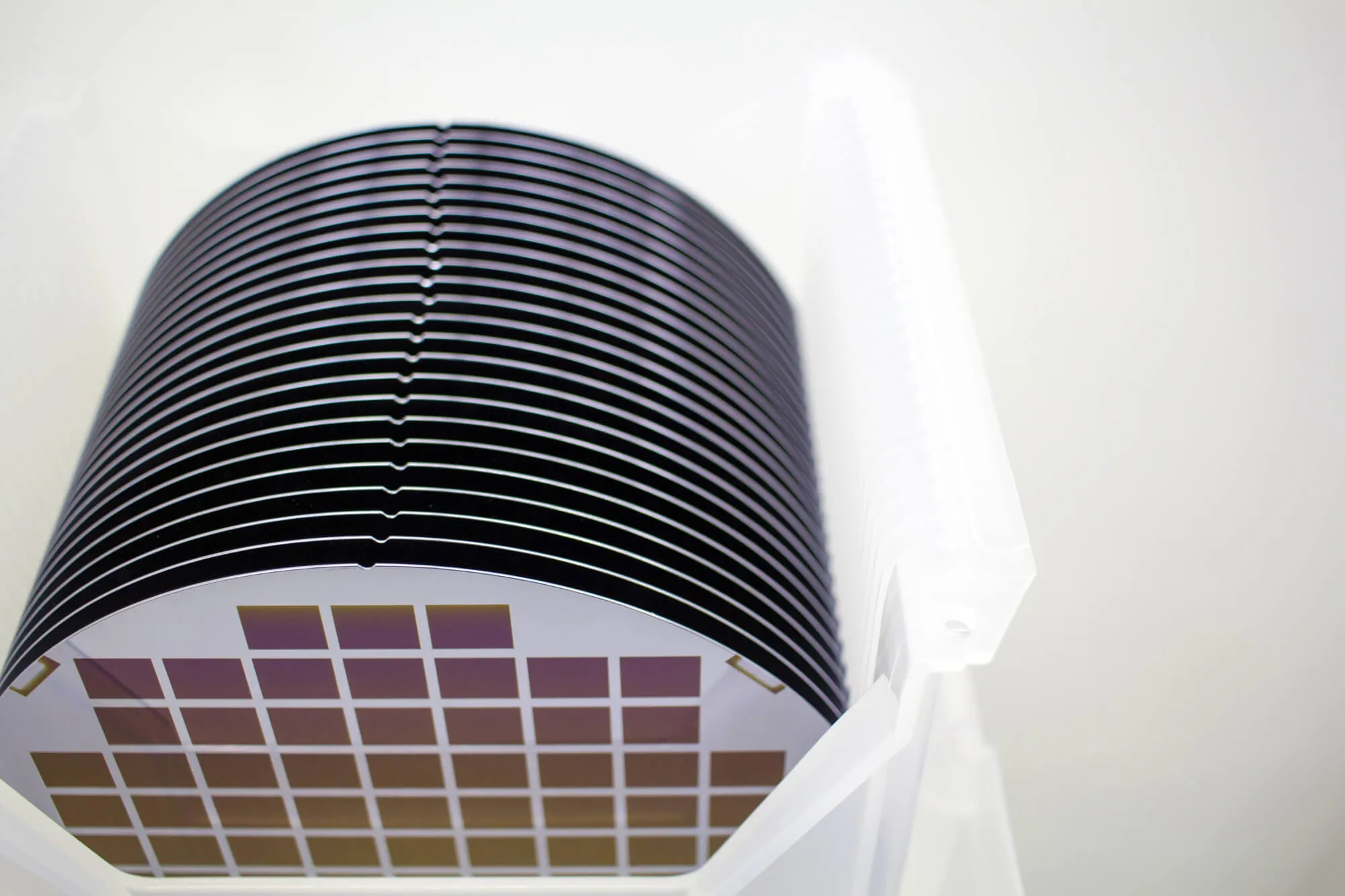
To produce a GaAs wafer, it must first go through material preparation to guarantee its quality. At Wafer World, we offer high-quality wafers at a reasonable price. Contact us for inquires!


