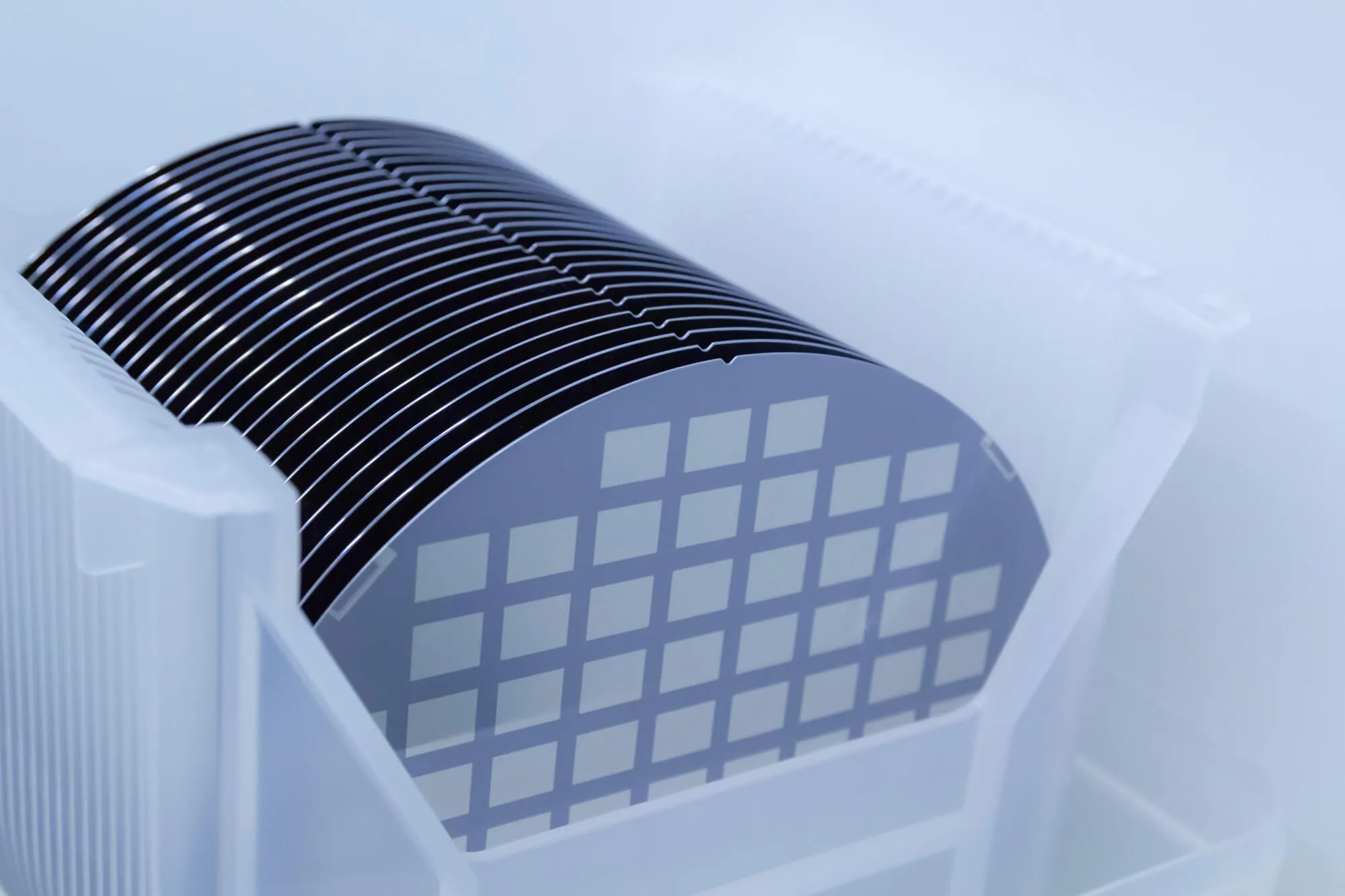
If you’re looking to find a type of wafer you can use in device manufacturing and double side patterning, you’ll want to learn more about the double side polish wafer. Due to its specific flatness, this wafer is also required in semiconductors and MEMs devices with low roughness and super flat specs. Wafers with reduced size and improved performance are in demand because their production cost is lesser than traditional wafers.

When it comes to silicon wafer manufacturing, wafer polishing plays a critical role. Aside from ensuring that the substrates are free from any sign of defects, the process also produces a thinner, stronger, and more pliable silicon wafer.
Polishing wafers involve the use of diamond liquid slurry, polishing pads, and a vacuum carrier. First, the vacuum carrier is used to hold the wafer in place while its backside is exposed.Next, it is gradually put in contact with a polishing pad that covers a rotating platen. Lastly, the damaged layers are carefully removed with the use of a calculated and precise force.
To achieve flatness while improving its levels of surface contamination, the substrate wafer has to be polished on both sides simultaneously or one side at a time. This double-side polishing method plays a significant role in reducing the roughness on the surfaces of the silicon wafer. However, it’s important to note that the manufacturer’s ultimate goal is to create a wafer that has the ability to maintain its extrinsic gettering capabilities.
When a wafer goes through the gettering process, its device-damaging contaminants that are found on its active circuit areas are taken away. As these metal impurities are being localized in the passive and predetermined parts of the substrate, they are significantly reduced.
Since a double side polish wafer offers top-quality surfaces on both its front and back regions, they’re the ideal choice for silicon on insulator fabrication, wafer bonding, microelectromechanical systems, and other products that require tight flatness.

At Wafer World, we produce high-quality wafers that suit your needs. Contact us today for inquiries!


