A crucial step in the process of making silicon wafers ready for reuse is the grinding and polishing process. Here are the basics of how this process is completed.

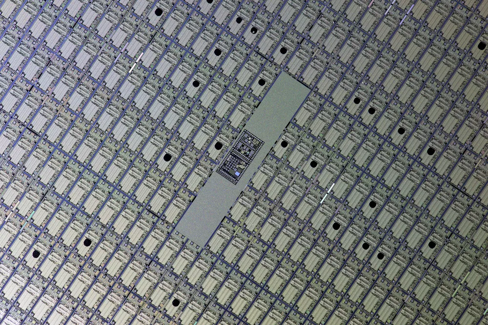
Carefully grinding silicon wafers down to thin and smooth them is a very technical process. By tinning wafers, they can also be reused and re-polished for future use. Back grinding is the conventional method for reducing wafers from their original thickness to a diminished thickness suitable for final packaging of die after dicing. Grinding is fast and also produces low variation and good surface finishes. For new, emerging applications that also use a very thin and ultra-thin die, grinding remains the common thinning method, but some process modifications and additional techniques are also required.
Using precise technology, wafers are ground down to incredibly thin levels. The delicate grinding wheels also employ graded diamond abrasives embedded in specially engineered binders on the wheel edge. The current production limit for grinding reduces wafers from an average starting thickness of 750 micrometers to as thin as 150 micrometers. Yield loss considerations from the grinding and downstream processes have also made it very difficult to thin below 150 micrometers in production. Research projects, on the other hand, are also consistently working below the 150 micrometers level and even 50 micrometers.
Wafer World is one of the best producers of new and refurbished silicon wafers on the market. Call today if you have any questions about our manufacturing process.


