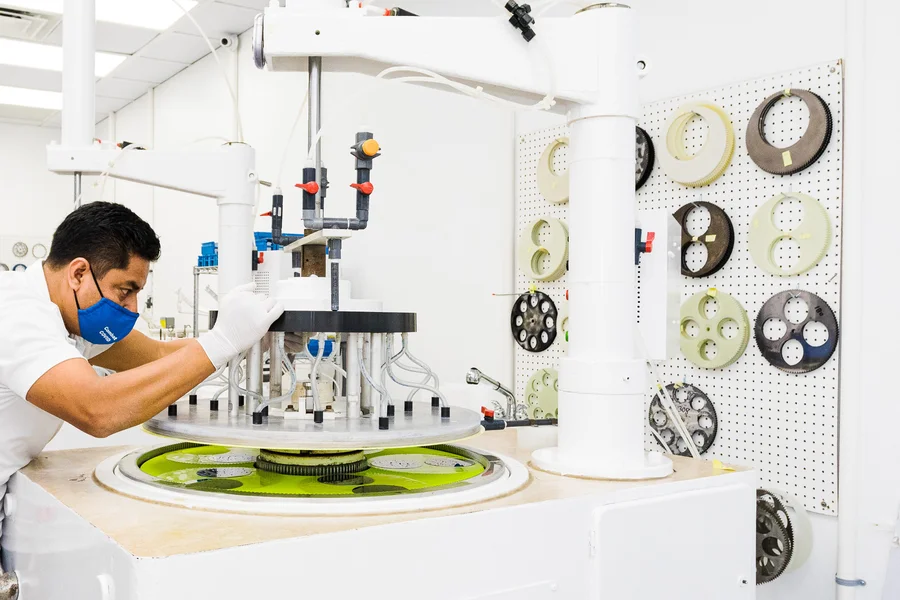
Not every silicon application asks for the same material properties. An FZ wafer is produced from float-zone silicon, a material associated with high purity and low concentrations of certain impurities because the molten silicon does not contact a crucible during crystal growth. Those characteristics make float-zone material useful in specialized industries where electrical behavior and substrate purity can carry significant importance.
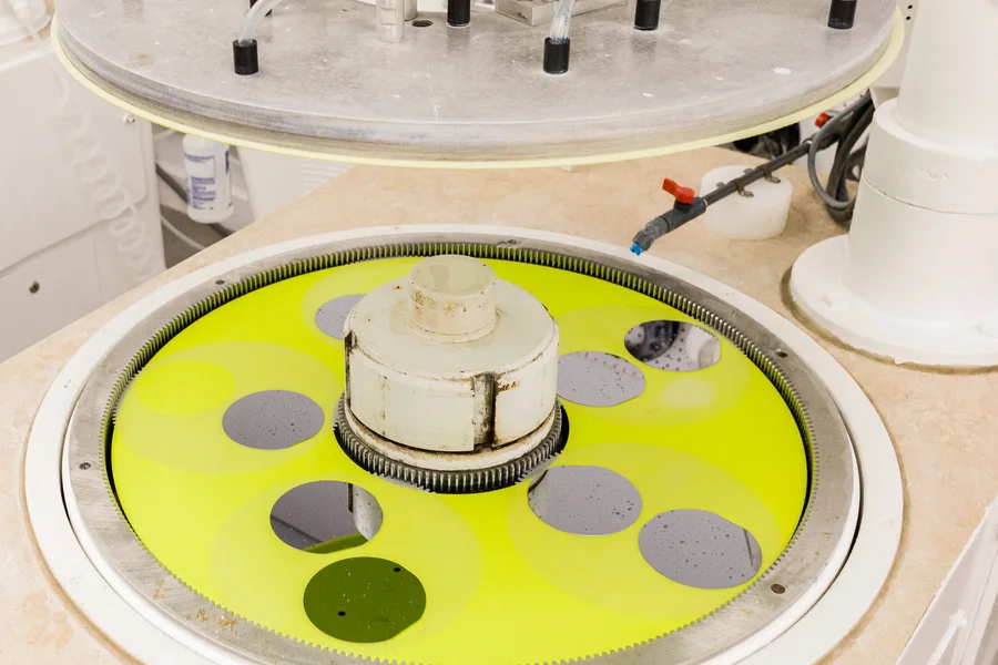
Power electronics is one of the established applications for float-zone silicon. Reference literature on semiconductor materials identifies the material as particularly important for high-power electronics and power rectifiers.
The float-zone process avoids contact between molten silicon and a container. This helps limit contamination, including oxygen introduced through crucible contact in other crystal-growth methods. Float-zone silicon can also be produced with high electrical resistivity, which is valuable for certain power semiconductor structures.
These properties help explain why the material is considered for devices designed to control or convert electrical power rather than being treated as a general-purpose substrate for every semiconductor product.
High-energy physics provides another important use case. CERN materials describe particle detectors as being commonly processed on high-resistivity float-zone silicon because detector substrates require high purity and high resistivity.
Silicon detectors convert interactions from incoming particles into measurable electrical signals. Substrate characteristics, therefore, become part of the detector design rather than simply a manufacturing detail.
Common reasons industries and laboratories evaluate float-zone material include:
The exact properties required still depend on the device, processing conditions, and intended operating environment.
Float-zone silicon also has a history in photovoltaic research. Published research has examined float-zone crystal growth for solar cells because minority charge-carrier lifetime can strongly influence the performance of semiconductor devices.
Float-zone growth can provide a useful platform for studying how defects and impurities affect photovoltaic behavior. Research reported in the Journal of Crystal Growth used high-purity float-zone silicon to isolate the effects of selected defects and impurities on photovoltaic properties.
This does not mean float-zone material is the standard choice for mass-market solar manufacturing. Its role is more specialized, particularly where researchers want carefully controlled material for experiments or advanced cell development.
Research laboratories also use float-zone silicon when studying fundamental semiconductor behavior. A highly pure starting substrate can help researchers distinguish the effects of intentionally introduced dopants, defects, processing steps, or irradiation from those caused by background impurities.
This makes the material useful for experiments involving carrier lifetime, radiation effects, impurity behavior, and device characterization. In these settings, selecting a substrate is part of controlling the experiment itself.
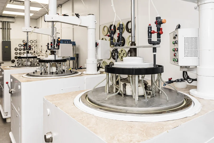
Choosing an FZ wafer begins with the application, followed by the material characteristics the device or research project actually requires. Wafer World can help you review available substrate specifications and discuss factors such as wafer dimensions, orientation, resistivity, doping, and surface requirements. Contact us to schedule a consultation or call to discuss the wafer specifications that fit your next project.




