.webp)
Stay up-to-date with the latest news and trends in wafer and semiconductor technologies.
*Blogs are for educational and informational purposes ONLY

Not all silicon wafer manufacturers work the same way. See what separates reliable suppliers from risky ones before you place an order.
Read More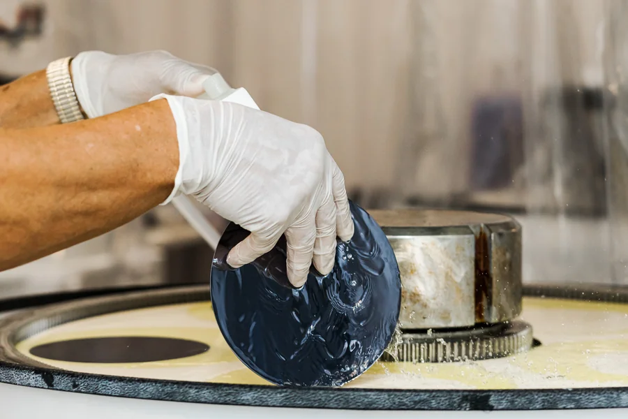
Curious how GaAs wafer differs from silicon in speed and efficiency? This guide breaks down the science, uses, and sourcing tips.
Read More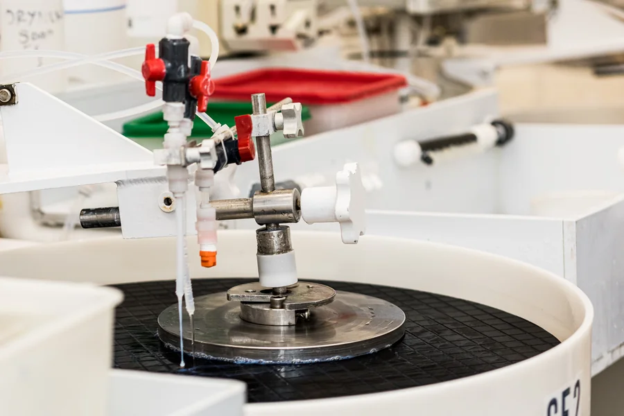
A Si wafer might look simple, but purity, doping, and finish can decide whether your entire semiconductor project succeeds or fails. Here's what actually matters.
Read More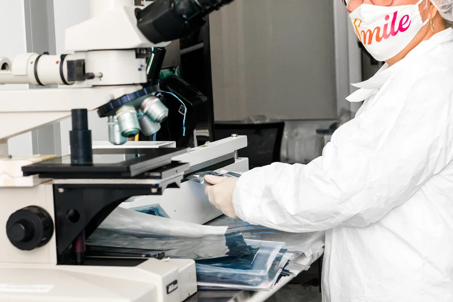
Explore how purity affects a float zone wafer, from oxygen concentration and crystal quality to resistivity needs and demanding electronic applications.
Read More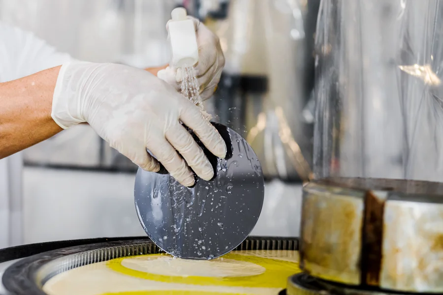
See how a double side polish wafer can improve thickness uniformity, surface flatness, process stability, and measurement consistency during fabrication.
Read More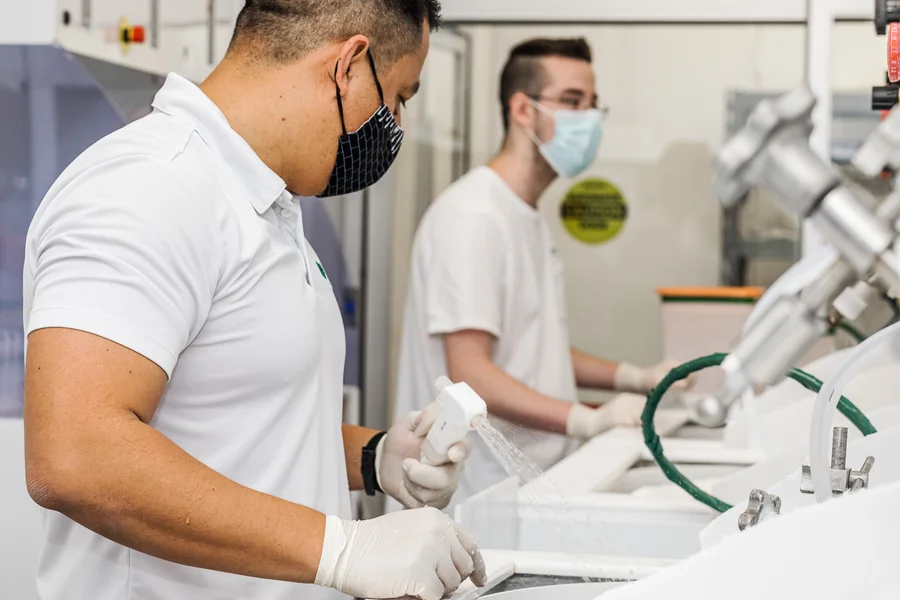
See what is shaping silicon prices in 2026, including global production, energy costs, trade exposure, demand shifts, and supply-chain conditions.
Read More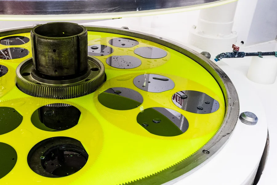
InP reclaim wafers can support advanced applications through careful evaluation of surface condition, dimensions, cleanliness, and reuse.
Read More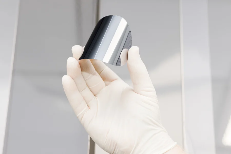
Crystal quality matters in an InP wafer, including how defects, lattice strain, and material uniformity can affect device performance.
Read More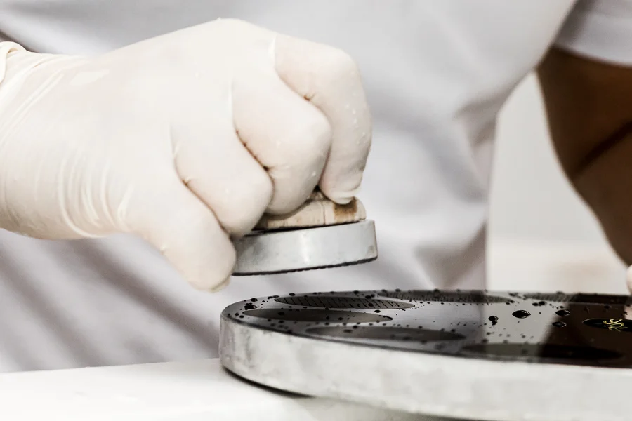
Explore key equipment used in silicon wafer manufacturing for crystal growth, wafer slicing, edge shaping, polishing, cleaning, and inspection.
Read More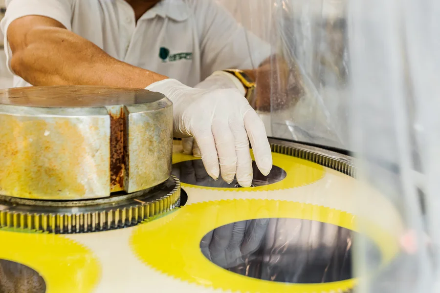
Explore how GaAs reclaim wafers are renewed through incoming inspection, layer removal, polishing, cleaning, and verification for suitable reuse.
Read More