GaAs reclaim wafers play a significant role in the semiconductor industry, offering unique advantages for various applications. However, addressing the challenges and exploring future directions is crucial to enhance their potential further. In this article, we will delve into the current challenges faced by GaAs reclaim wafer technology and discuss the promising future directions that researchers and industry experts are pursuing.
Defects can significantly impact GaAs reclaim wafers’ quality and performance. Surface roughness, crystallographic defects, and dislocation density are among the types of defects that pose challenges in achieving defect-free reclaim wafers. Moreover, researchers diligently work to minimize flaws through advanced fabrication techniques, process optimization, and material selection. Understanding the root causes of defects and developing effective mitigation strategies can improve the quality and performance of GaAs reclaim wafers.
Defect engineering is crucial in reducing crystallographic defects in GaAs reclaim wafers. Techniques such as strain relaxation strategies, lattice mismatch compensation, and dislocation filtering are being explored. These methods aim to minimize flaws and improve the crystalline quality of the wafers.
Additionally, advanced characterization techniques, including transmission electron microscopy (TEM) and atomic force microscopy (AFM), enable researchers to identify and analyze defects at the nanoscale level, facilitating targeted defect reduction efforts.
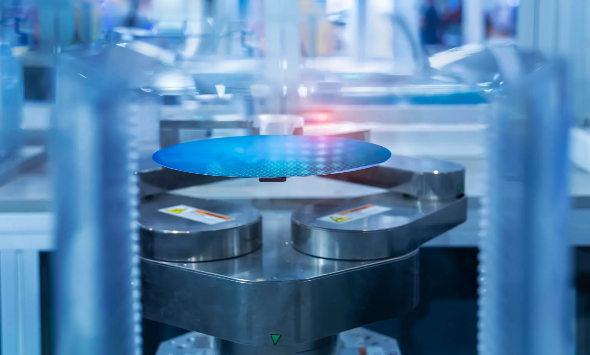
Epitaxial lift-off (ELO) and chemical mechanical polishing (CMP) are commonly used to fabricate GaAs reclaim wafers. However, these techniques have their limitations. ELO can be time-consuming, while CMP may introduce new defects during polishing. Consequently, researchers are exploring novel approaches and integrating advanced fabrication techniques to improve yield, efficiency, and the overall manufacturing process. These techniques include the following:
Laser lift-off techniques offer advantages such as higher throughput and reduced material wastage compared to traditional ELO methods. By utilizing laser-induced stress, the epitaxial layers are separated from the substrate, enabling the reclaiming of GaAs wafers.
On the other hand, plasma etching techniques allow precise control over material removal, enabling the fabrication of ultra-thin and defect-free GaAs reclaim wafers.
Wafer bonding techniques are being investigated to achieve strong and reliable bonding between the reclaimed GaAs wafers and other substrates, expanding their integration possibilities.
Larger wafer sizes offer numerous advantages, including higher throughput, improved productivity, and reduced manufacturing costs per unit area. However, scaling up the wafer size for GaAs reclaim wafers presents technical challenges. The crystal quality, wafer bowing, and strain management become more critical as the wafer size increases. For this reason, researchers are investigating new growth techniques, substrate engineering, and process optimization to implement larger wafer sizes successfully.
One approach to address the challenges associated with larger wafer sizes is the development of improved growth techniques such as metalorganic vapor phase epitaxy (MOVPE) and molecular beam epitaxy (MBE). These techniques enable better control over the growth parameters, improving crystal quality and reducing strain in larger GaAs reclaim wafers. Additionally, substrate engineering techniques involving patterned or graded substrates can alleviate wafer bowing issues, ensuring the flatness and uniformity of larger wafers.

Combining GaAs reclaim wafers technology with other semiconductors or substrates opens up exciting device integration and performance enhancement possibilities. Researchers are investigating the benefits and challenges of integrating GaAs reclaim wafers with materials such as silicon, germanium, and other III-V compound semiconductors. This integration can lead to synergistic applications, enabling the development of advanced devices with enhanced functionalities, such as hybrid optoelectronic systems, photovoltaics, and high-speed electronics.
The integration of GaAs reclaim wafers with silicon, known as silicon-on-gallium arsenide (Si-on-GaAs), offers the potential to combine the high electron mobility of GaAs with the mature fabrication processes and scalability of silicon technology. This integration can result in the development of these high-performance devices, which are critical for wireless communication systems:
Leveraging the advantages of both materials allows researchers to achieve improved device performance, reduced power consumption, and enhanced integration density.
Integrating GaAs reclaim wafers with other III-V compound semiconductors, such as indium phosphide (InP) or gallium nitride (GaN), opens doors to various applications. For instance, combining GaAs reclaim wafers with InP enables the realization of these high-speed photonic devices for optical communication systems:
Likewise, integrating GaAs reclaim wafers with GaN enables the development of power devices and high-frequency electronics for applications in power electronics, radar systems, and satellite communications.
Researchers are also exploring incorporating two-dimensional (2D) materials, such as graphene or transition metal dichalcogenides (TMDs), with GaAs reclaim wafers. These 2D materials offer unique properties, including high carrier mobility, optical transparency, and mechanical flexibility. Combining these materials with GaAs reclaim wafers helps researchers develop novel device architectures for the following:
To meet the ever-increasing demands of high-performance devices, researchers focus on enhancing the performance of GaAs reclaim wafers in various aspects. Higher electron mobility and energy efficiency are critical for radio frequency (RF) and microwave device applications, where low noise, high gain, and high-frequency operation are essential.
Improving the crystalline quality, reducing defects, and optimizing the doping profiles allow researchers to achieve higher electron mobility. These performance enhancement methods enable them to develop high-speed transistors, power amplifiers, and low-noise amplifiers.
It’s crucial to Improve uniformity and crystalline quality for optoelectronic devices such as light-emitting diodes (LEDs), laser diodes, and photodetectors. By reducing crystal defects, strain, and non-uniformity across the wafer, researchers can enhance the performance and efficiency of these devices, leading to improved optical communication systems, solid-state lighting, and high-speed optical interconnects.
Researchers are exploring new materials and their compatibility with GaAs reclaim wafers to unlock additional potential and enable the development of innovative device architectures.
For instance, integrating quantum dots or quantum wells with GaAs reclaim wafers can develop highly efficient, tunable, and low-power-consuming devices, such as single-photon emitters, quantum sensors, and next-generation solar cells.
.webp)
Get in touch with Wafer World today and explore our extensive collection of top-notch wafers crafted to suit the unique demands of your industry. Our experienced team is eager to provide detailed insights into our exceptional product line. Don't miss out on the opportunity to enhance your operations. Contact us now to discover the possibilities.


