
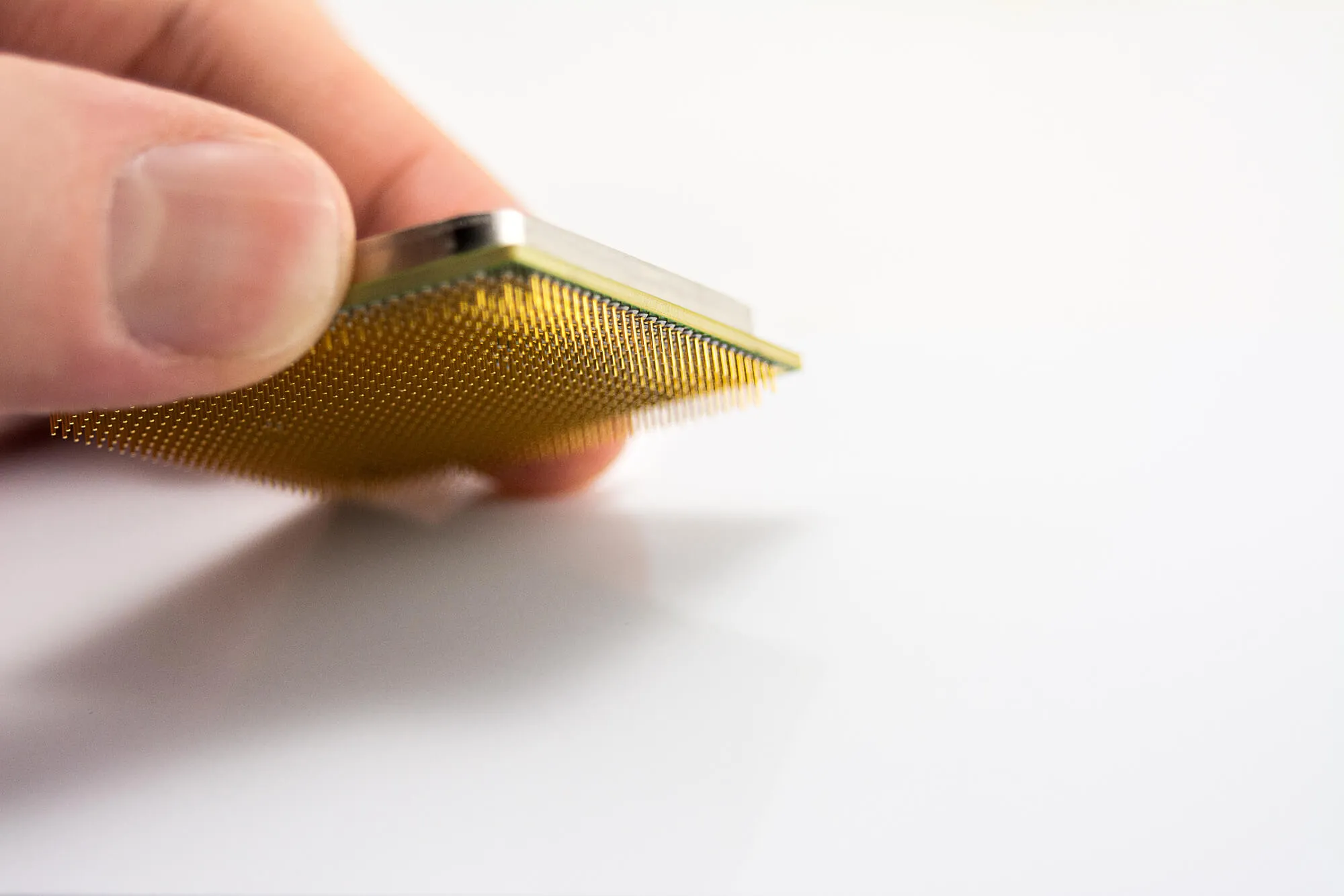
In semiconductor manufacturing, double-sided polish wafers have emerged as a critical component, playing a vital role in producing high-quality devices. This article delves into the significance of double-sided polish wafers, their manufacturing process, and their impact on the advancement of semiconductor technology.
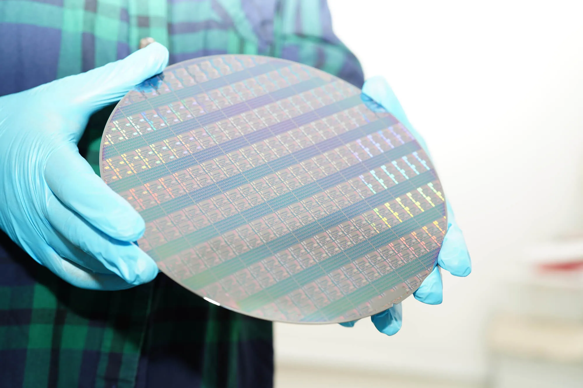
Double-sided polish wafers are meticulously engineered substrates in semiconductor manufacturing. These wafers possess exceptional flatness and surface quality, ensuring precise device fabrication. The importance of flatness and surface quality cannot be overstated, as they directly influence the performance and reliability of electronic components.
The manufacturing process of double-sided polish wafers involves several steps to achieve the desired flatness and surface quality. This includes initial wafer preparation and cleaning, followed by mechanical grinding and polishing techniques to remove imperfections. Chemical-mechanical planarization (CMP) achieves uniformity and smoothness across the wafer surface. Rigorous inspection and quality control measures ensure the final product meets the required standards.
This wafer offer numerous advantages in semiconductor manufacturing. These wafers' enhanced flatness and reduced thickness variation enable precise device fabrication. The improved surface quality and reduced defect density result in higher device yield and improved performance. Double-sided polish wafers are crucial in enhancing the efficiency and reliability of semiconductor device manufacturing.
Double-sided polish wafers find applications in various semiconductor industry sectors. They are integral to the fabrication of integrated circuits and microelectronics, providing the foundation for high-performance electronic devices. In optoelectronics and photonics, double-sided polish wafers enable the production of advanced devices such as lasers and photodetectors. Additionally, they are vital in developing MEMS (Microelectromechanical Systems) and sensors, ensuring precise and reliable operation.
The production of double-sided polish wafers presents challenges. Consistently maintaining thickness and flatness across the entire wafer requires precise control and advanced manufacturing techniques. Uniform material removal during the CMP process is crucial to achieving the desired surface quality. Ongoing innovations in polishing materials and techniques contribute to further improvements in manufacturing efficiency and quality.
Double-sided polish wafers are poised to contribute to future advancements in silicon semiconductor technology. As miniaturization continues and advanced device structures are developed, the demand for high-quality wafers with exceptional flatness and surface quality will increase. Integrating emerging technologies like artificial intelligence and the Internet of Things will require specialized double-sided polish techniques tailored to specific application requirements.
At Wafer World, our team can provide high-quality silicon wafers, germanium, and other materials to help your business grow. Give us a call to learn more about the products we offer!


