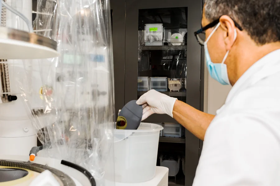
A wafer may look smooth and clean to the naked eye, but semiconductor manufacturing operates at a scale where tiny surface irregularities and contaminants can matter. During silicon wafer processing, cleaning and polishing help prepare the surface for later fabrication steps by addressing particles, residues, roughness, and unwanted surface damage. These preparation stages are closely connected because polishing creates the desired surface condition, while cleaning removes materials that should not remain.
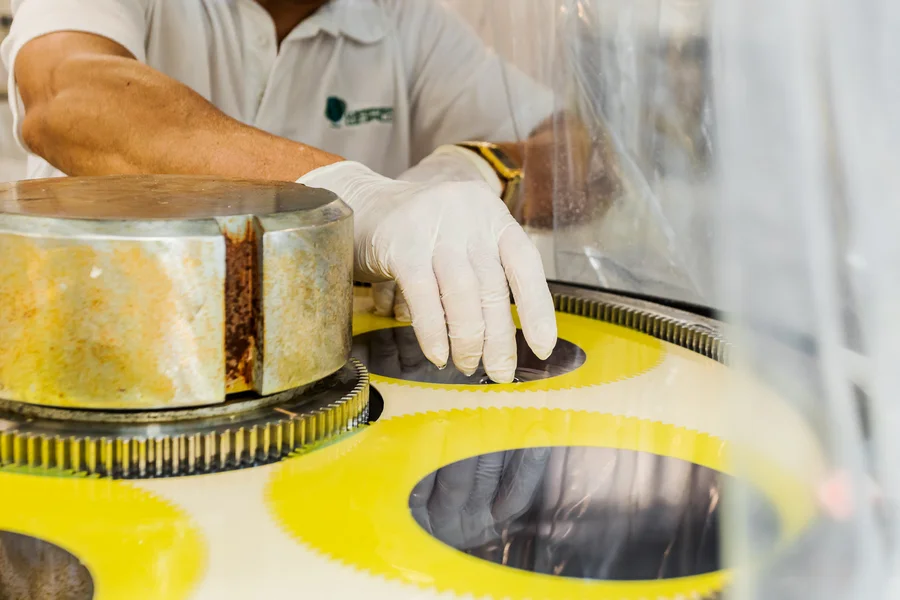
Semiconductor fabrication builds structures through repeated processing steps. That makes the starting surface important. According to the Semiconductor Industry Association, chemical mechanical planarization uses chemical and physical forces to flatten wafer surfaces so they are ready for subsequent circuitry layers.
For silicon substrates, polishing also has an important preparatory role before device fabrication begins. NIST publications describe polishing as a means of removing mechanical surface damage and producing a highly flat, mirror-finished surface suitable for later processing.
A polished surface is not simply about appearance. Surface topography can influence how effectively subsequent processes interact with the wafer. Better flatness provides a more uniform foundation for operations that depend on controlled surface conditions.
Polishing can help:
The result is a surface that is better suited to demanding downstream manufacturing steps.
Polishing improves surface condition, but the process can also leave particles or residues behind. NIST notes that post-CMP cleaning equipment is specifically designed to remove particulate residue resulting from chemical mechanical polishing. This illustrates why polishing and cleaning should be viewed as connected stages rather than isolated tasks.
Particles, organic material, and metallic contamination are important considerations when preparing semiconductor surfaces. Historical NIST guidance identifies these as common categories of wafer contamination and notes that particles generated during polishing can interfere with later processing.
Cleaning, therefore, serves a practical quality-control purpose. The objective is to remove unwanted material without undermining the surface condition established during polishing. Depending on the manufacturing process, cleaning methods may be selected to address particular contaminants and material requirements.
Surface quality depends on more than achieving a polished appearance. A wafer can be flat yet carry unwanted residue, while a clean wafer can still have surface damage or unsuitable topography. Coordinating both processes helps address these different quality factors before the substrate advances.
Inspection and metrology add another layer of control. The Semiconductor Industry Association explains that inspection tools can evaluate characteristics such as wafer thickness, alignment, and defects during manufacturing. These measurements help manufacturers identify problems before additional layers and processes increase the consequences of an unsuitable surface.
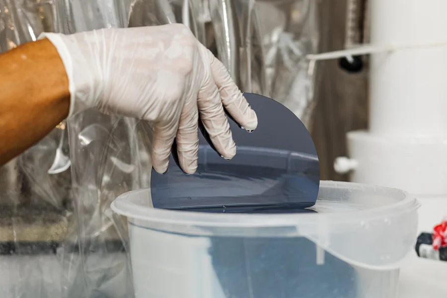
Cleaning and polishing deserve careful consideration whenever surface condition, contamination control, and consistency are important to silicon wafer processing. Wafer World can help you discuss your substrate requirements and determine suitable wafer options for your application. Contact us to schedule a consultation and discuss the wafer characteristics your process requires.




