October 14, 2023
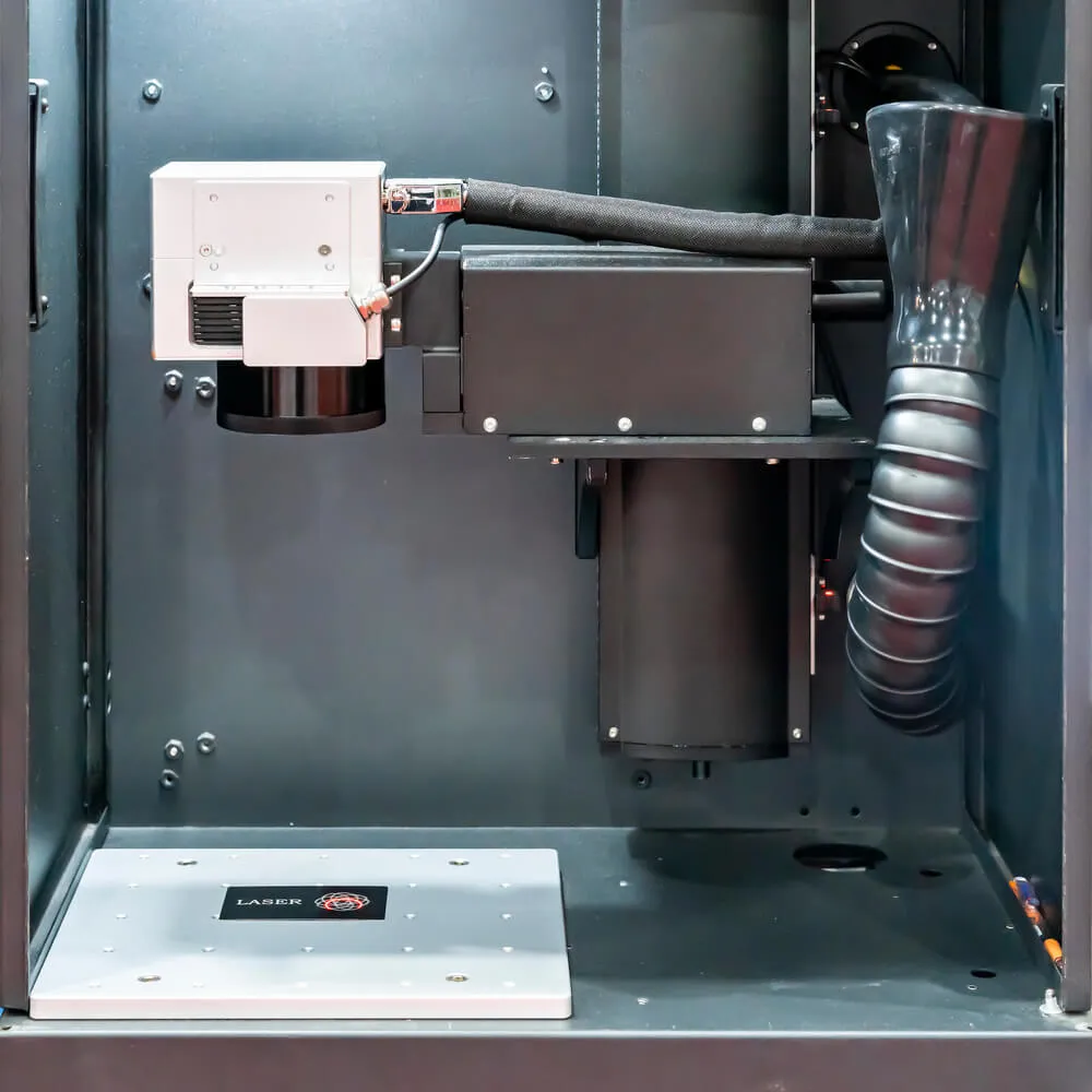
Shop NowThe semiconductor industry is a cornerstone of modern technology, powering everything from smartphones to laptops and electric cars. It's an industry that thrives on precision and innovation, and laser marking has become an integral part of semiconductor manufacturing processes. Laser marking offers high precision and speed when labeling and engraving semiconductor components. However, while it brings undeniable benefits to the industry, it's crucial to assess its environmental impact.
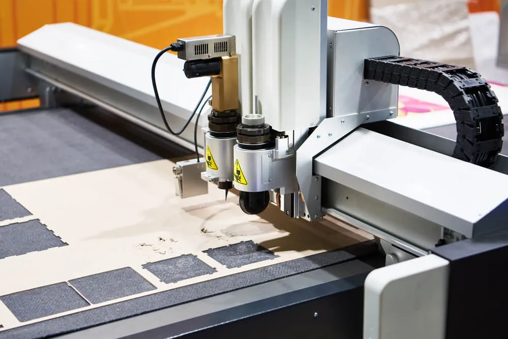
Before delving into the environmental impact of laser marking, it's essential to understand why it's so widely adopted in the semiconductor industry. Laser marking offers several advantages over traditional marking methods such as chemical etching or ink printing.
To evaluate the environmental impact of laser marking in the semiconductor industry, we need to consider several factors:
Laser marking systems require electricity to operate, and the energy consumption can vary depending on the type of laser used and the complexity of the marking. However, compared to some other manufacturing processes, laser marking is relatively energy-efficient. Newer laser systems are designed with energy-saving features and technologies, further reducing their environmental footprint.
One of the potential environmental benefits of laser marking is the reduction in materials usage. Traditional methods like chemical etching often involve the use of hazardous chemicals and solvents, which can be harmful to both the environment and worker health. Laser marking eliminates the need for these chemicals, contributing positively to environmental sustainability.
Waste generation is a crucial factor to consider when evaluating the environmental impact of any manufacturing process. Laser marking generates minimal waste, as it's a non-contact process that removes material in a controlled manner. Additionally, the waste generated is often in the form of small metal or ceramic particles, which can be easier to recycle compared to chemical waste from traditional methods.
Emissions from laser marking can vary depending on the type of laser used and the materials being marked. Some lasers produce minimal emissions, while others may emit small amounts of particulate matter or gases. Semiconductor manufacturers need to choose laser systems that are designed with emissions control and mitigation measures to minimize their environmental impact.
When assessing the environmental impact of laser marking, it's crucial to consider the entire lifecycle of the equipment. This includes manufacturing, transportation, and disposal. Manufacturers can reduce their environmental footprint by choosing energy-efficient equipment, sourcing materials responsibly, and implementing recycling and disposal programs for obsolete laser systems.

The semiconductor industry is not oblivious to the importance of environmental sustainability. Manufacturers are continuously seeking ways to reduce their environmental impact while maintaining high-quality production. Several advancements in laser marking technology contribute to these efforts:
Ultra-fast pulsed lasers, such as picosecond and femtosecond lasers, have gained prominence in semiconductor manufacturing due to their unique advantages. These lasers produce extremely short pulses of high-intensity light, enabling precise and efficient marking without significant heat generation. This reduced heat minimizes the risk of damaging delicate semiconductor components, leading to higher yield rates and less material waste.
Laser ablation is a technique that involves removing material from a surface through laser-induced vaporization. Advancements in laser ablation technology have focused on achieving near-zero residue. This means that when a semiconductor component is laser-marked, there is little to no material left behind, further reducing waste generation and the need for post-processing cleaning steps.
Modern laser marking systems come equipped with advanced software that optimizes the marking process for minimal environmental impact. These software solutions allow for precise control over laser parameters, ensuring that the least amount of energy is used to achieve the desired marking result. Additionally, they can optimize the path of the laser beam to minimize unnecessary markings and reduce material removal.
While laser marking offers undeniable advantages in terms of precision, speed, and materials reduction, it's crucial to approach its use in the semiconductor industry with a commitment to environmental responsibility. Here are some steps that can be taken to mitigate the environmental impact further:

Laser marking has become an indispensable tool in the semiconductor industry, offering precision and efficiency that traditional methods struggle to match. While it brings numerous benefits, it's essential to acknowledge its environmental impact. By adopting energy-efficient technologies, minimizing waste generation, and implementing recycling programs, semiconductor manufacturers can continue to advance their industry while reducing their environmental footprint. Ultimately, Wafer World’s commitment to environmental responsibility can ensure a sustainable future for both the semiconductor industry and the planet. Call us today!


