In the world of modern technology, where gadgets and devices dominate our lives, silicon wafers and chips are the unsung heroes that power these marvels. Silicon wafers and chips are at the heart of nearly every electronic device we encounter, from smartphones to computers to advanced medical equipment. But have you ever wondered about the journey these components undergo, from raw materials to the final product?
In this article, we'll dive into the fascinating world of manufacturing silicon wafers and chips, exploring the intricate differences between these two essential components.
Silicon wafers serve as the canvas upon which the intricate microstructures of semiconductor devices are etched. These wafers start their journey as raw silicon ingots, which are cylindrical blocks of high-purity crystalline silicon. The process of transforming these ingots into polished, ultra-flat wafers involves several key steps.
While the Czochralski method is a common approach for growing silicon ingots, other methods like the Float-Zone method are also employed. The Float-Zone method involves melting the tip of a silicon rod and slowly pulling it upwards, producing highly pure silicon wafers used in specialized applications like solar cells and high-power devices.
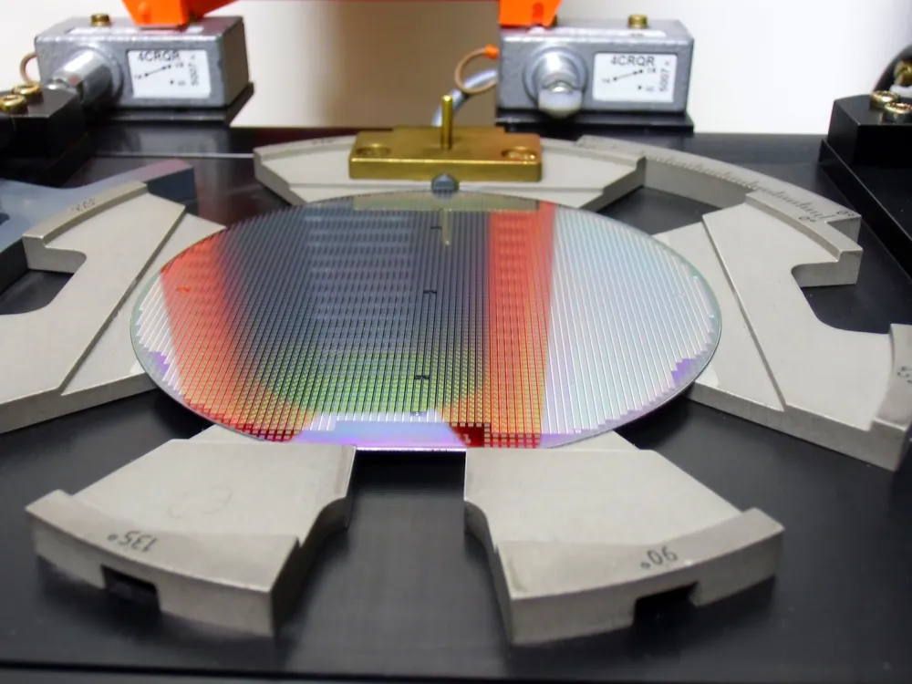
Over the years, the diameter of silicon wafers has increased to accommodate more chips per wafer, thereby improving efficiency and lowering costs. From the early 2-inch wafers, we now have wafers with diameters of 12 inches or more, allowing for higher chip production in a single batch.
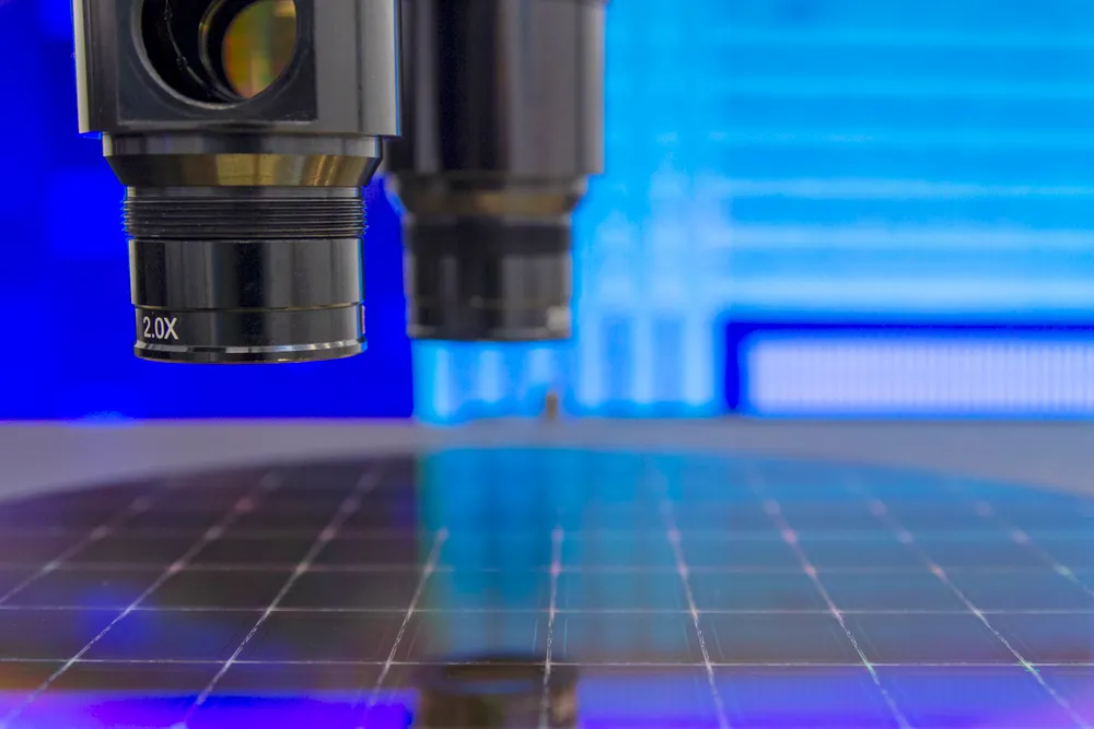
The precision of wafer flatness and surface quality is critical. Advanced techniques like atomic force microscopy (AFM) and interferometry are used to measure and characterize the surface topography down to nanometer scales.
Various cleaning and contamination control processes are employed to ensure the wafers are free of impurities, particles, and residues that can adversely affect chip performance. This involves using chemicals, gases, and controlled environments to maintain high cleanliness standards.
The crystal lattice structure of silicon must be highly uniform to achieve optimal semiconductor properties. Various techniques, including seeding and controlled cooling, are used to promote the formation of a single crystal structure.
Additional thinning processes are employed for applications requiring thin wafers. This can involve mechanical grinding, chemical mechanical polishing (CMP), or even innovative techniques like laser-assisted thinning to achieve the desired wafer thickness.
Each wafer is tracked using unique identifiers, allowing manufacturers to trace its journey throughout the fabrication process. This traceability aids in quality control, defect detection, and process optimization.
Due to the delicate nature of silicon wafers, sophisticated handling and automation systems are in place to minimize the risk of contamination, breakage, and other forms of damage.
In cases where chips are damaged, or production yields are suboptimal, wafer reclamation and recycling techniques are employed to recover materials and reduce waste.
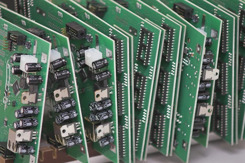
Chips, also known as integrated circuits or microchips, are the final products that emerge from the silicon wafer manufacturing process. These chips can range from simple logic gates to highly sophisticated microprocessors. The process of manufacturing chips involves intricate steps that build upon the foundation laid by silicon wafer production.
A meticulous design optimization phase takes place before a chip's physical fabrication begins. Engineers analyze the functionality, power consumption, heat dissipation, and physical layout of the chip's components to ensure optimal performance and efficiency.
As chip designs have become more intricate, traditional photolithography techniques have faced limitations in achieving the desired resolution. Double patterning and multi-patterning methods are employed to overcome this. These techniques involve multiple exposures and chemical processes to achieve finer features on the chip.
Traditional planar transistors were once the norm, but as technology scaled down, they encountered leakage and power consumption issues. This led to the development of FinFET (Fin Field-Effect Transistor) and 3D transistor technologies. These designs involve three-dimensional structures that enhance control over the current flow, leading to better performance and energy efficiency.
As chip features continue to shrink, even more precise lithography methods are required. EUV lithography utilizes extremely short wavelengths of light to create smaller and more intricate patterns on the silicon wafer, enabling the fabrication of advanced chips with nanometer-scale features.
CVD plays a vital role in depositing thin films of various materials onto the wafer's surface. This process involves introducing gaseous reactants into a chamber, chemically reacting and forming solid layers on the wafer. CVD is essential for creating insulating and conducting layers that make up the chip's intricate circuitry.
CMP is used to planarize the chip's surface, ensuring uniformity across the wafer. This step is crucial to avoid irregularities that can affect the performance of the chip's various components.
Metrology and inspection techniques are employed throughout the chip manufacturing process to verify the accuracy of dimensions, alignments, and structures. Advanced tools such as scanning electron microscopes (SEM) and optical inspection systems are used to catch defects and ensure quality.
Not all chips on a wafer may turn out fully functional due to defects or manufacturing variations. Yield enhancement techniques involve identifying and mitigating these defects, often through redundancy or advanced error correction methods, to increase the overall yield of functional chips.
From humble raw materials to sophisticated electronic components, the journey of manufacturing silicon wafers and chips is a tale of precision, innovation, and complexity. Silicon wafers lay the foundation upon which chips are built, serving as the canvas for intricate microstructures. On the other hand, chip manufacturing transforms these wafers into our devices' brains, where complex circuitry and cutting-edge technologies converge.
Wafer World continues to push the boundaries of technology, and the collaboration between these two processes remains integral to shaping the future of electronics. Call us today!


