February 6, 2020
Shop NowTo prevent wafer defects, such as cracking and chipping, silicon wafer manufacturing standards have required the polishing of wafers, especially in the bevel region. During etching, some of the etched materials are deposited on the bevel or backside of the wafer. This accumulation of debris and particles can cause defects, which often leads to yield loss. In this article, we will discuss to you the three different types of wafer defects created during the etching stage.

During silicon wafer manufacturing, peeling and particle defects can occur in so many ways. The films deposited during manufacturing cover the edge, the bevel area, as well as the apex of the wafer. But it affects the edges the most; removing some stacks, since the following dry etches are not isotropic. This means that the remaining pile of films can experience interfacial stress that hampers them from uniting properly. During the heating and cooling process, these interfacial stresses together with material property change can degrade the film’s ability to adhere to each other, leading to the formation of a scar. This scar can grow further through thermal expansion. The wet etching process can also add further damage by bombarding the fragile surfaces of the wafer’s edge, leading to delamination.
Arcing refers to the electrical disintegration of a gas that generates an extended electrical discharge. Unbalanced charge distribution in low dielectric insulating layers during an increased condition ratio RIE can cause arcing damage to occur. Arcing damage mostly takes place near metallization lines, which will then act as a ground route to active areas in the dielectric insulating layer.
Micromasking defects develop at the bevel area if the etched material is exposed at the bevel during the etching step. They are detected during high aspect ratio etch processes.

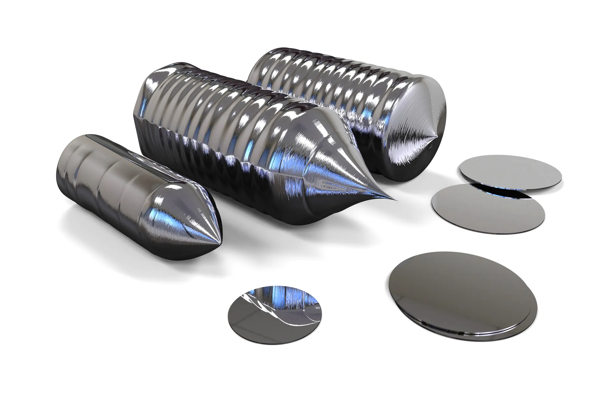
Get high-quality silicon wafers from a trusted silicon wafer manufacturing. At Wafer World, we offer high-quality silicon wafers at a sensible price. Contact us for inquires or purchase wafers online!


