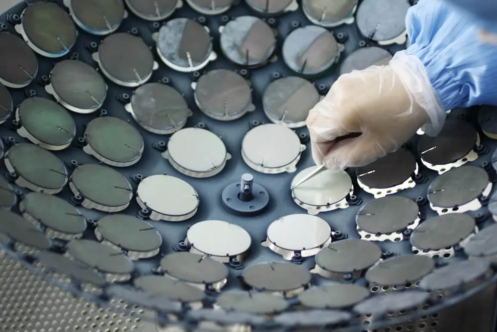
Float zone wafers, also known as FZ wafers, are single-crystal silicon slices that have been produced using the float zone method. This specialized manufacturing technique offers several advantages, making them invaluable in a wide range of high-tech applications. In this blog post, we delve into why they are an essential component in various industries.
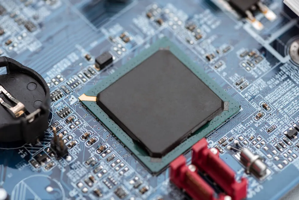
The semiconductor industry is one of the principal applications for float zone wafers. FZ wafers are great substrates for fabricating sophisticated microchips and integrated circuits due to their high purity and defect-free crystal structure. Controlling the doping process precisely throughout wafer manufacture ensures consistent and dependable performance, increasing the efficiency and speed of electrical devices.
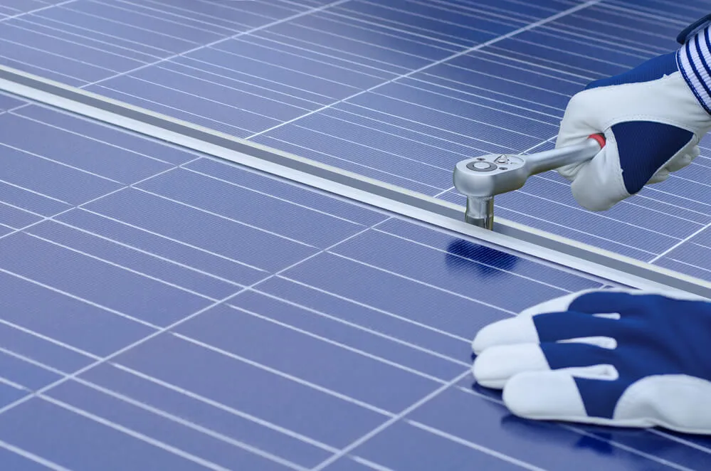
Float zone wafers are widely employed in the production of solar cells. The high-quality crystal structure and low impurity levels boost solar cell conversion efficiency greatly. As a result, FZ wafers are a popular alternative for manufacturing high-performance photovoltaic cells used in solar panels, contributing to the global trend toward renewable energy sources.
Power devices, such as insulated gate bipolar transistors (IGBTs) and high-voltage diodes, require substrates that are both durable and stable. These needs are met by float zone wafers, which have outstanding electrical qualities that allow for effective power management and increased performance in electric vehicles, renewable energy systems, and industrial applications.
Light-emitting diodes (LEDs) and laser diodes, for example, require high-purity substrates to work optimally. FZ wafers' defect-free crystal structure enables minimum non-radiative recombination, resulting in improved light emission efficiency, color accuracy, and longer device lifespans.
MEMS devices, which are used in a variety of sensing and actuating applications, need precise and stable substrates. Float zone wafers provide the mechanical stability and high surface quality required for the fabrication of MEMS sensors, accelerometers, and microfluidic systems.
Float zone wafers are at the forefront of innovative technology, playing an important role in a wide range of applications across multiple industries. Their high purity, crystal structure, and electrical qualities help to enhance semiconductors, renewable energy, power electronics, optoelectronics, and MEMS. As technology advances, the need for float zone wafers is expected to rise. You can contact Wafer World to become a part of this technical advancement and improve your business in the future!


