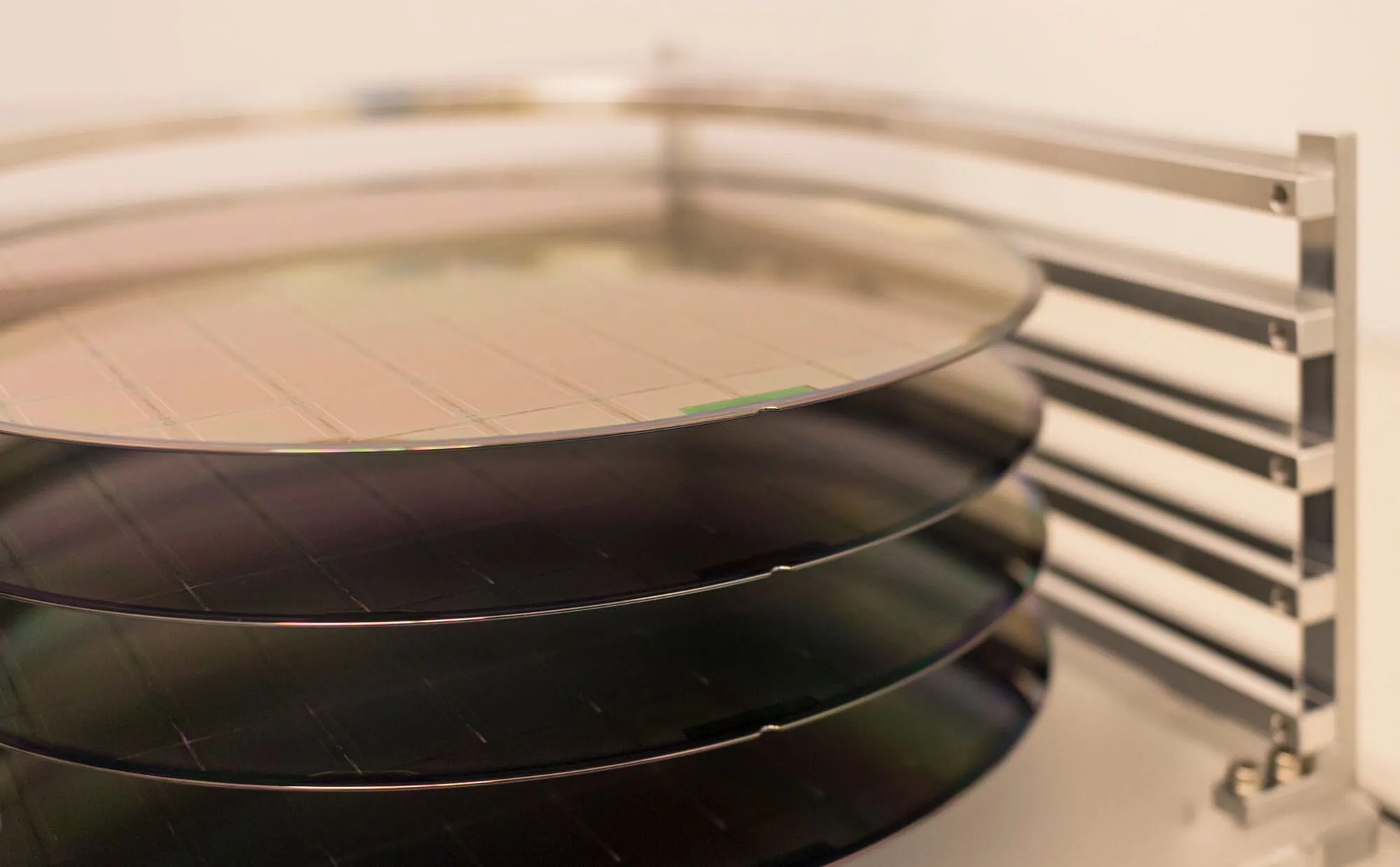
Gallium arsenide or GaAs wafers are semiconductor materials with unique qualities such as fast electron mobility and low noise. They are perfect for various applications, including solar cells, high-speed transistors, and microwave-integrated circuits. Despite their benefits, GaAs wafers can be costly and have lesser heat conductivity than other materials
As a result, researchers are constantly looking for innovative ways to improve the characteristics and performance of GaAs wafers. In this article, we'll look at some of the most recent advancements in GaAs wafer technology and the future of this interesting subject.
https://www.youtube.com/watch?v=tdxvsEShmc0
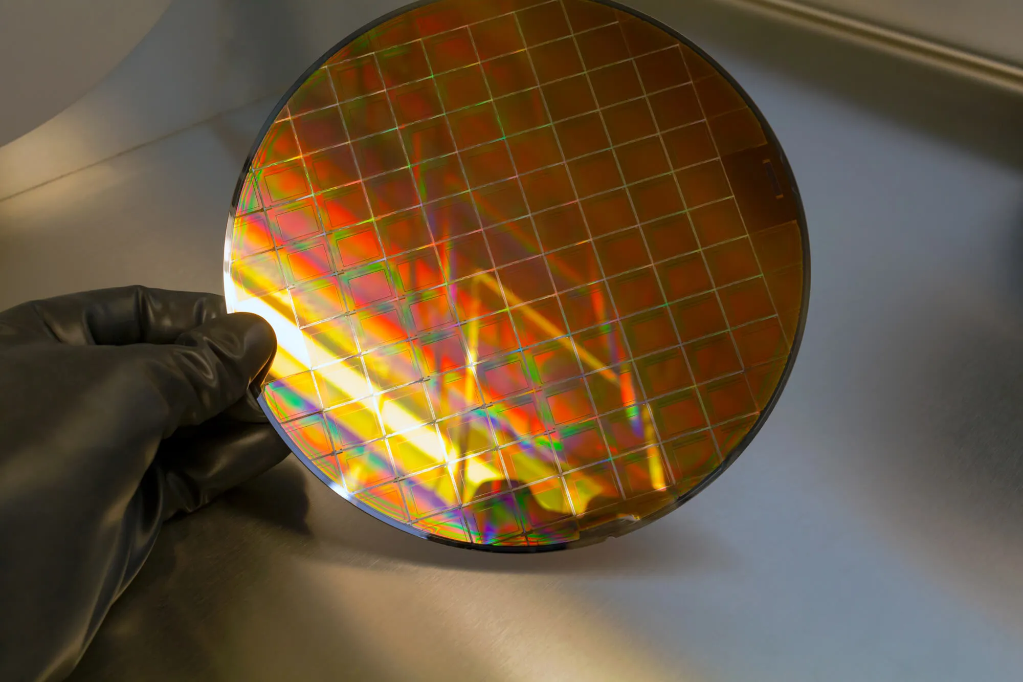
GaAs wafers are used in various applications, including satellite communication systems, photovoltaic devices, and lasers. They are well-known for their high electron mobility and efficiency in converting light to electrical energy, making them suitable for use in solar cells.
On the other hand, GaAs wafers are more expensive than other semiconductor materials, limiting their use in particular applications. Furthermore, GaAs wafers have lesser heat conductivity than other materials, making them more difficult to utilize in some high-power applications.
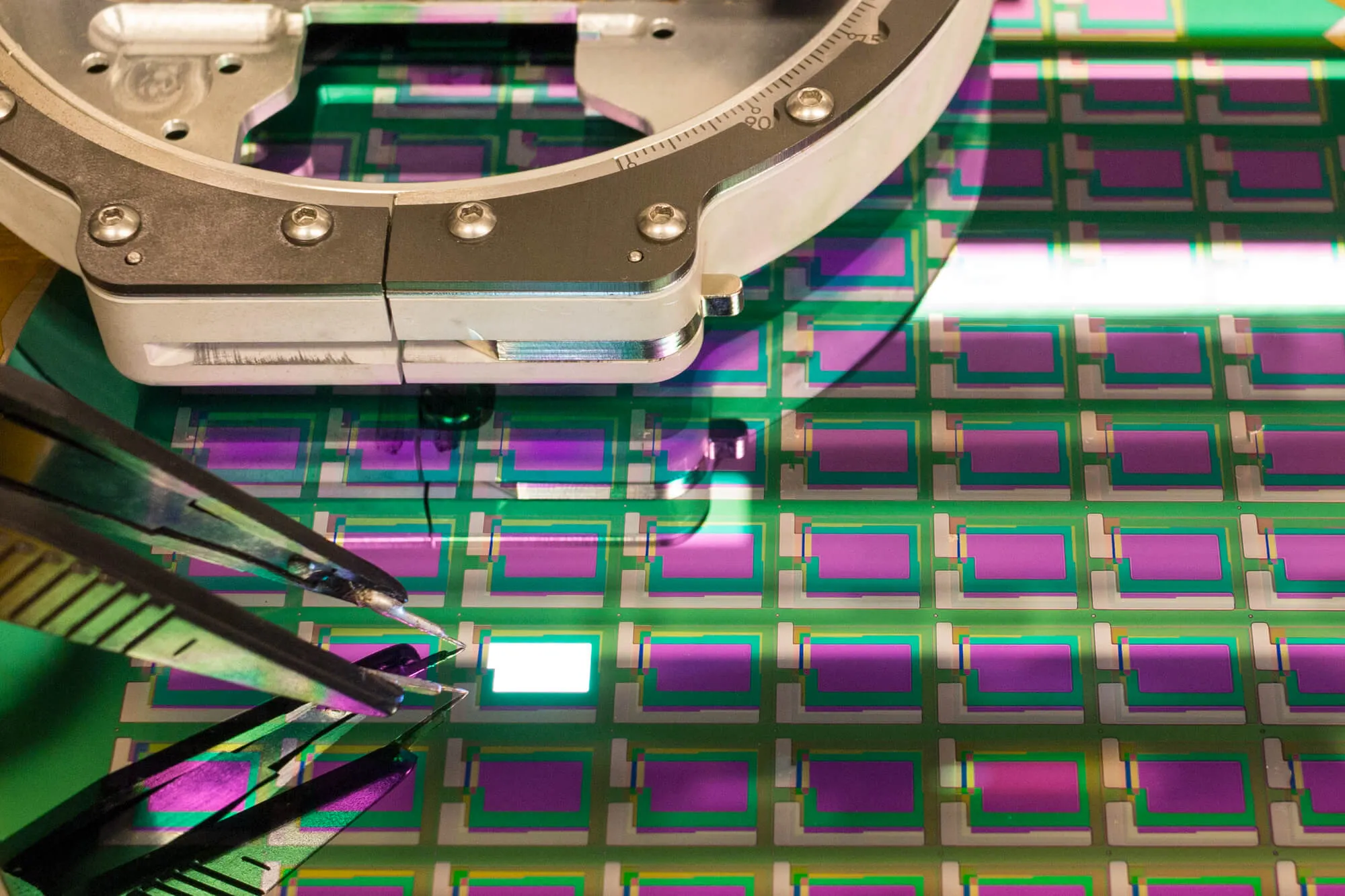
The fabrication processes for GaAs wafers are complex and involve several steps. The following is a general overview of the key steps involved in the fabrication of GaAs wafers:
Despite these obstacles, researchers are constantly looking for new ways to improve the characteristics of GaAs wafers and broaden their range of applications. New growth processes, wafer property improvements, and applications are among the most recent advancements in GaAs wafer technology.
Developing new growing methods for GaAs wafers is one area of active study. Molecular Beam Epitaxy (MBE), Metalorganic Vapor Phase Epitaxy (MOVPE), and Liquid Phase Epitaxy are now the most prevalent methods for growing GaAs wafers (LPE). However, researchers are investigating novel strategies to increase the growth rate, lower costs, and improve the quality of the resultant wafers.
One potential approach is III-V molecular beam epitaxy (MBE), a more accurate and regulated method of manufacturing GaAs wafers. This approach deposits materials onto the wafer surface using a combination of solid-state and gas-phase precursors, resulting in a more uniform and controlled growth process. Furthermore, researchers are working on creating novel low-cost, high-volume growth technologies that can be used to create GaAs wafers more efficiently and cheaply.
Another aim of GaAs wafer research is the creation of wafers with superior attributes, such as increased electron mobility, noise performance, and thermal conductivity. Increasing GaAs wafer electron mobility is essential for high-speed transistors and high-frequency applications. Several researchers are investigating the usage of nanowires to improve the electron mobility of GaAs wafers by reducing electron scattering when electrons flow through the material.
Increasing the thermal conductivity of GaAs wafers is also a key difficulty because these wafers do not dissipate heat as well as other materials. One possible option is to include other materials, like diamond or silicon carbide, within the GaAs wafers, which have higher thermal conductivity and can help to dissipate heat more efficiently.
Finally, researchers are looking into novel uses for GaAs wafers, including quantum devices, high-speed communication systems, optoelectronics, and photonic devices. GaAs-based quantum devices are particularly intriguing since they have the potential to allow novel computer and communication technologies. Researchers are investigating using GaAs wafers to construct quantum dots, microscopic particles that can store and process quantum information.
GaAs-based high-speed communication systems are also being studied, as GaAs wafers can fabricate high-speed transistors and other components required for high-bandwidth communication systems. Furthermore, GaAs wafers are employed in developing optoelectronics and photonic devices that may transform light into electrical signals or vice versa.
While the future of GaAs wafer technology is attractive, some major hurdles must be overcome. Integrating GaAs wafers into current electronic systems is one of the most common difficulties. Because GaAs wafers are incompatible with standard silicon-based electronic systems, new integration methods must be developed to be widely used.
While novel growth methods seem promising, it will be necessary to scale up manufacturing to fulfill the increasing demand for GaAs wafers in various applications. Notwithstanding these obstacles, the future of GaAs wafer technology is bright. With further research and development, we may anticipate new and fascinating applications for GaAs wafers in the next years. Furthermore, the ability to create low-cost, high-volume growth processes for GaAs wafers may make them a more realistic option for various applications.
GaAs wafer technology is a fascinating and fast-expanding industry with numerous prospects for growth and advancement. With continued research into new growing processes, wafer property improvements, and the development of new applications, we may expect GaAs wafers to be used in an increasingly varied range of applications. While there are obstacles to overcome, the potential benefits of GaAs wafer technology make it a field of research worth investigating further.
At Wafer Word, we provide our customers with valuable information about our products. Contact us today to learn more about our services!


