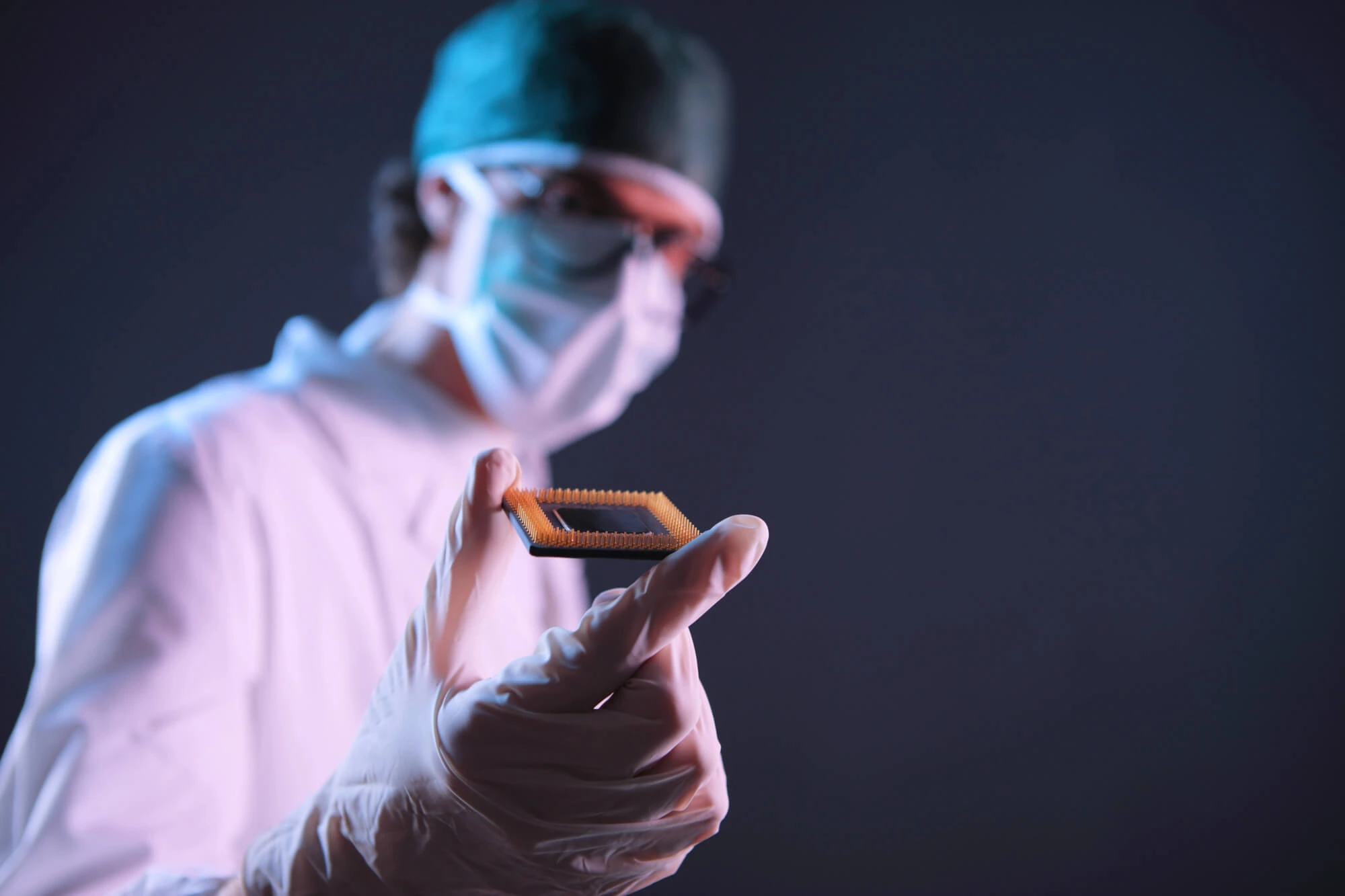
Wafer bonding is a critical technology in semiconductor manufacturing. It enables the integration of materials that would otherwise be difficult or impossible to combine using conventional epitaxial growth or deposition techniques. For a GaAs wafer, this process opens a world of new possibilities in device fabrication, such as heterogeneous integration, high-efficiency optoelectronic components, and advanced RF devices.
If you’re considering GaAs wafer bonding for your project, understanding the principles, available methods, and key challenges is key to ensuring performance and product yield.
Wafer bonding involves joining two semiconductor wafers together so that their surfaces adhere on an atomic or molecular level. This bond will then have to withstand subsequent processing steps such as thinning, etching, and high-temperature annealing, so it’s key that it’s strong.
There are various wafer bonding techniques, including:
Each method has specific advantages depending on the materials involved, bonding temperature constraints, and the intended device structure.
GaAs is a III-V compound semiconductor known for its superior electronic and optoelectronic properties. Unlike traditional silicon, GaAs offers advantages such as:
Because of these features, GaAs is widely used in high-speed devices, light-emitting diodes (LEDs), laser diodes, solar cells, and RF amplifiers.
However, GaAs substrates are expensive and brittle, making efficient use and integration critical. Wafer bonding offers a path to transfer thin GaAs layers onto cheaper, more robust substrates or to stack dissimilar materials in 3D architectures.
As mentioned, there are various methods for bonding gallium arsenide substrates. Some of these include:
Two ultra-flat, clean surfaces are brought into contact in direct bonding, and a high-temperature annealing step (typically 300–600°C) converts this into a stronger covalent bond.
Direct bonding with GaAs wafers presents some challenges. For instance, this substance is more chemically reactive than silicon. Native oxides on the surface prevent strong bonding, so proper preparation by removing them using techniques like wet etching or plasma cleaning, for instance, is crucial.
Thermal expansion mismatch with common substrates like Si can introduce stress or defects during annealing. Luckily, low-temperature bonding helps avoid thermal mismatch issues but may yield weaker bonds.
Adhesive bonding involves an intermediate polymer layer between the GaAs wafer and the target substrate, such as benzocyclobutene (BCB), SU-8, or polyimide.
This method's benefits include compatibility with low-temperature processing and tolerance to surface roughness and particle contamination. Additionally, adhesive bonding allows for a flexible choice of bonding partners (like GaAs to Si, glass, or metal).
Sadly, the intermediate layer may degrade under high temperatures or radiation, so it’s not ideal for extreme applications. Moreover, this method may limit thermal dissipation and electrical conductivity.
In this method, a thin metal layer is deposited on both wafers, which are then joined under pressure and heat to form a thermocompression or eutectic bond. Metal-assisted bonding is used in applications such as:
Some advantages include a strong mechanical bond and the potential for electrical and thermal conduction across the interface. However, metal layers must be carefully chosen during the process to avoid interdiffusion or oxidation.
In plasma-activated bonding, a low-temperature plasma (usually O₂, Ar, or N₂) activates wafer surfaces, increasing their hydrophilicity and surface energy. This method facilitates bonding at lower temperatures (below 300°C), which is especially valuable for GaAs.
Plasma-activated bonding is compatible with CMOS back-end-of-line (BEOL) processes and helps reduce the risk of damage to fragile GaAs wafers.
Besides the mentioned applications, some uses of GaAs bonded wafers include:
Wafer bonding enables the monolithic integration of GaAs-based optoelectronic devices (such as lasers or photodetectors) onto silicon photonics platforms. This combination leverages the cost-effectiveness and maturity of Si technology with the performance advantages of GaAs.
GaAs layers can be bonded onto other III-V materials to form tandem solar cells with efficiencies exceeding 40%. Wafer bonding allows the stacking of different bandgap materials to capture a broader solar spectrum.
GaAs active layers can be transferred to transparent or flexible substrates to create thin-film light sources. Wafer bonding followed by substrate removal (etching or grinding) enables this structure.
GaAs is ideal for high-frequency RF applications. Wafer bonding allows GaAs-based active devices to be integrated with passive silicon components or heat-spreading substrates.
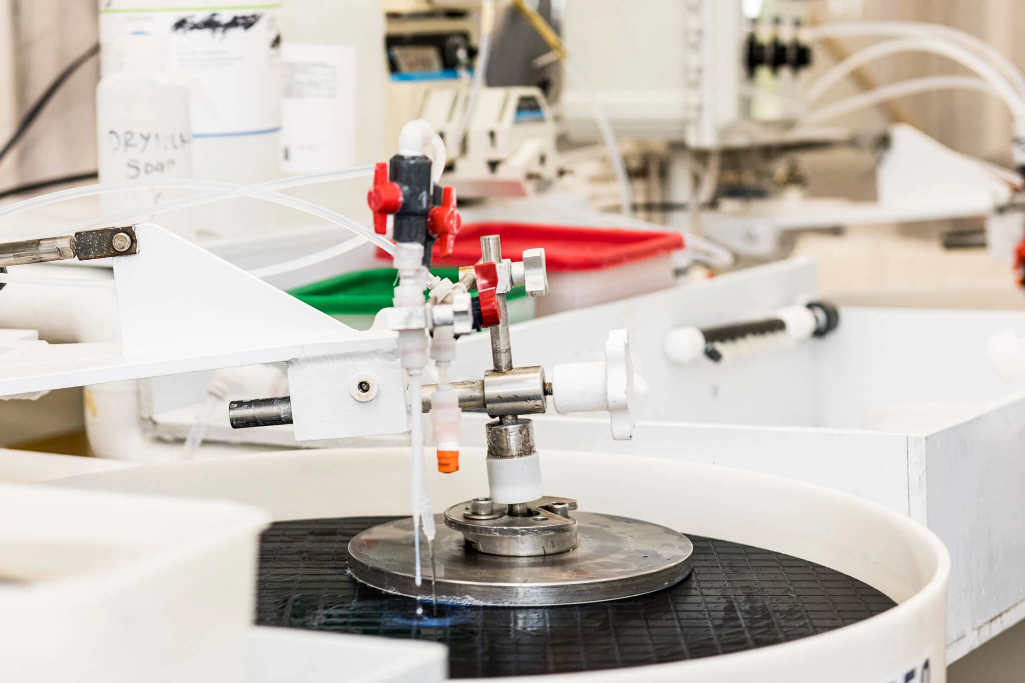
Achieving atomically smooth, clean surfaces is critical for successful bonding. To achieve that, manufacturers must conduct:
GaAs and Si, for example, have different coefficients of thermal expansion (CTE). High-temperature processes can lead to delamination or cracking, so low-temperature bonding and stress management techniques (like using buffer layers) are essential.
Maintaining uniform bond strength across the entire surface is a challenge, especially for large-diameter wafers. Void formation due to particles or trapped gases can degrade device yield.
After bonding, processes like substrate thinning, etching, or lithography must be performed without damaging the bonded structure. The choice of bonding method often dictates which post-processing steps are feasible.
Wafer bonding is a powerful tool for advancing the capabilities of GaAs-based devices by enabling heterogeneous integration, reducing costs, and supporting novel architectures. Successful GaAs wafer bonding hinges on careful surface preparation, precise alignment, and thermal management, whether through direct bonding, adhesive bonding, or metal-assisted methods.
As demand for high-performance optoelectronics, RF devices, and integrated photonics continues to grow, wafer bonding will play a pivotal role in bringing GaAs closer to mainstream silicon technologies, making high-performance semiconductor systems more efficient and versatile.
If you need high-quality GaAs wafers for your project, contact Wafer World today!


