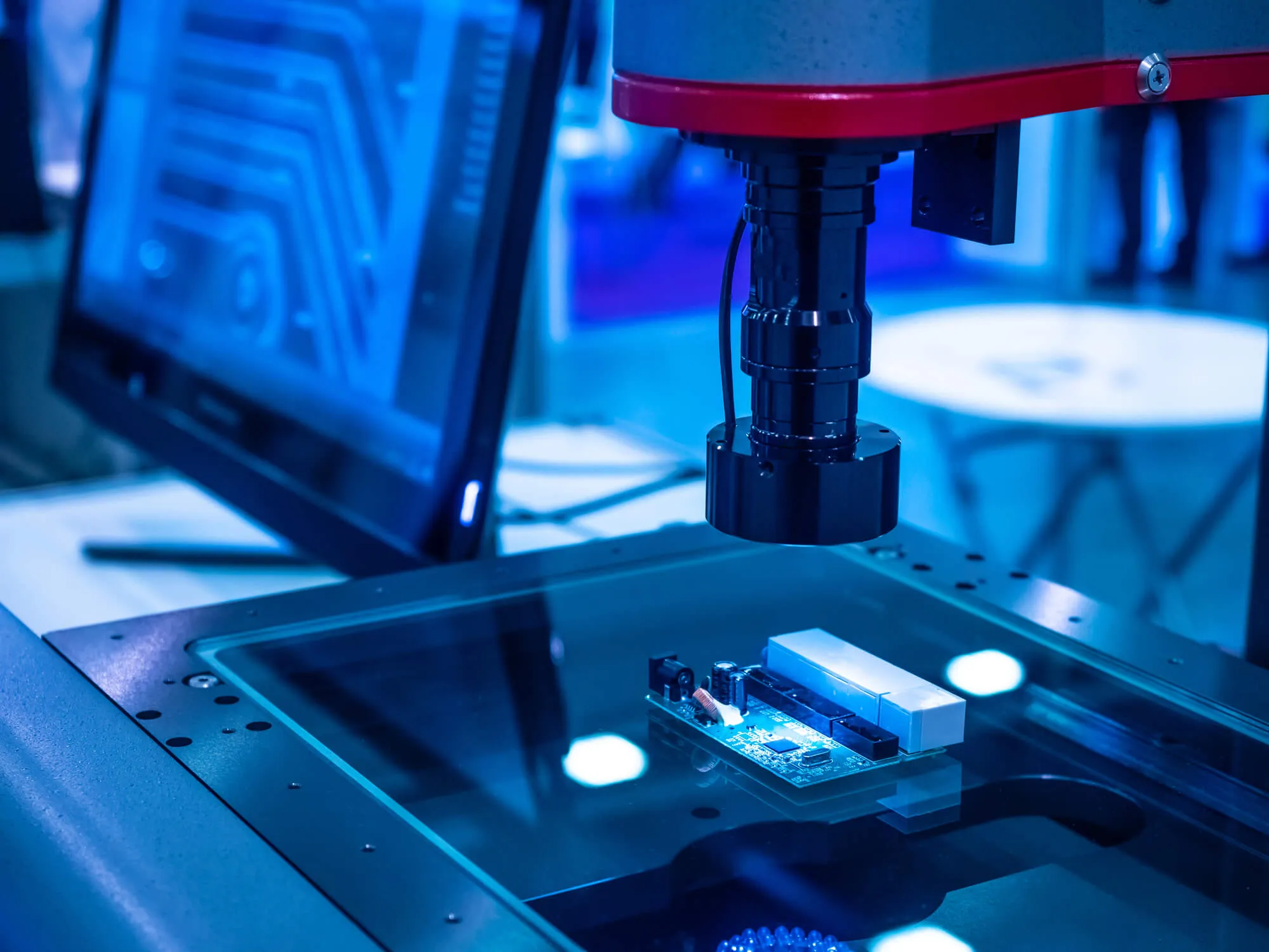
As our technology becomes more advanced, it also seems to get smaller. Just looking at the components of a cell phone, computer, or television and how they’ve changed over the last 30 years paints a drastic picture of the break-neck pace of technology. As our electronic devices become smaller, so do the semiconductors that allow them to work, which means that the manufacturing process has had to adapt. Laser marking has been one of those necessary adaptions. There’s an entire world that goes into creating wafer semiconductors, and one of the least explored elements of this process is the role of lasers and laser marking. Wafer World is here to shed some light on how lasers are crucial in making the semiconductors that make much of our modern technology possible.

The word ‘laser’ is actually an acronym that stands for light amplification by stimulated radiation emission. These devices create highly-concentrated beams of light by constantly stimulating and adding more energy to weak like waves until they grow in intensity. This is done through a series of lenses that amplify the emission until it creates a coherent light source in a narrow beam that retains its form across broad distances. Depending on the application and type of device, lasers' power can be modulated, which makes them useful for a wide range of applications. Lasers can be used on large sheets of metal or to make tiny markings on sensitive equipment, making them perfect for semiconductor manufacturing.
The two most common types of lasers used for marking this kind are near-infrared (NIR) and green lasers. Although they are both well-suited for the task, they have some fundamental differences. Historically, NIR lasers have been the most commonly used, but the new generation of green lasers is starting to gain some traction.
Near-infrared lasers are extremely versatile, making them well-suited for many machine applications like semiconductor creation. They are effective because of the energy range that falls squarely within the spectral field needed to make wafers' necessary markings.
Green lasers are the result of second-harmonic generation processes, also called frequency doubling. In simple terms, this technology combines two photos to make a new one with twice the energy. This amplifies the power while conserving the coherence of the laser.
There are two main reasons why the laser marking process is important: traceability and readability.
The main reason wafers are marked, so they are easily tracked throughout the manufacturing process. Semiconductors go through many steps before they are finally ready to be distributed. This includes polishing, cleaning, and testing. During this progression, it’s important to differentiate between the different wafers so that each one undergoes the necessary procedures and those that don’t meet the standards can be separated.
Different semiconductors have different applications. Laser marking is a useful way of denoting which item is suitable for different uses. Lasers not only cut into the surface of a wafer, but they can also re-arrange the surface particles, creating marks that are minutely shallow yet easily readable.

There are two different types of laser marks used on semiconductors; etched markings and annealed markings.
For etched markings, lasers are used to remove thin layers of material, leaving behind a textured mark of about 12 to 25 microns deep. These are often referred to as ‘hard marks’ because there is a visible change in the surface layers.
For annealed markings, the lasers are set to a lower power level, so the laser re-arranges the molecules rather than etching the surface. This creates a contrast on the surface that is visible when the wafer reflects light.
Lasers are perfect for making the needed marks and cuts during the semiconductor manufacturing process because of the many variables they address:
Many of the elements used to make semiconductors are quite sensitive. This is especially true for silicon wafers. These components' surface can be seriously distorted by even the slightest miscalculation, which means that using specialized cutting devices can compromise the areas adjacent to the cuts. This issue is avoided with lasers. Furthermore, the energy beam is so precise and can be modulated to exert the exact amount of energy needed to make cuts by removing material without dispersion. Lasers can make the mark without causing damage.
As we mentioned, semiconductor surfaces can be susceptible, and some areas can be influenced or changed when others are manipulated. Lasers maintain a stable power output throughout the marking process, which makes the procedure consistent. This avoids drastic changes in the depth of the marking, which can compromise the structure of the semiconductor.
Lasers emit a stable and concentrated beam of light that can be adjusted to the desired narrowness. This light can be used for tiny applications while providing a precise cut with little to no variability, even down to the smallest units of measurements.
Lasers provide effective markings while limited mistakes. Part of the reason this is possible is because the process is automated. This eliminates the human factor and substantially reduces the likelihood of errors.
There are no chemicals associated with laser markings. The process simply uses light to achieve the desired result, and they do not require very much electricity to work. This makes laser markings energy-efficient and fairly safe for the environment.
Both etching and the molecular alternation alternatives for laser marking leave a permanent mark on the wafers. This means that the semiconductors can be tracked and identified not only during manufacturing but for years to come.

Every part of the semiconductor manufacturing process is important for creating a high-quality result. As one of the industry leaders, Wafer World is your resource for all things wafer semiconductors. Keep it on the site to learn more or get in touch to request a quote today!


