Silicon wafers are the heart and soul of modern electronics. From microchips to solar cells, these thin slices of silicon play a crucial role in enabling the technologies we rely on every day. But have you ever wondered about the intricate process involved in creating these essential components? Today, we'll dive and uncover the key steps that make it all possible.
The journey begins with the creation of a high-purity silicon crystal, which serves as the foundation for silicon wafers. Through a process called the Float-Zone, a single crystal is grown, carefully controlling the cooling and solidification to ensure a uniform lattice structure.
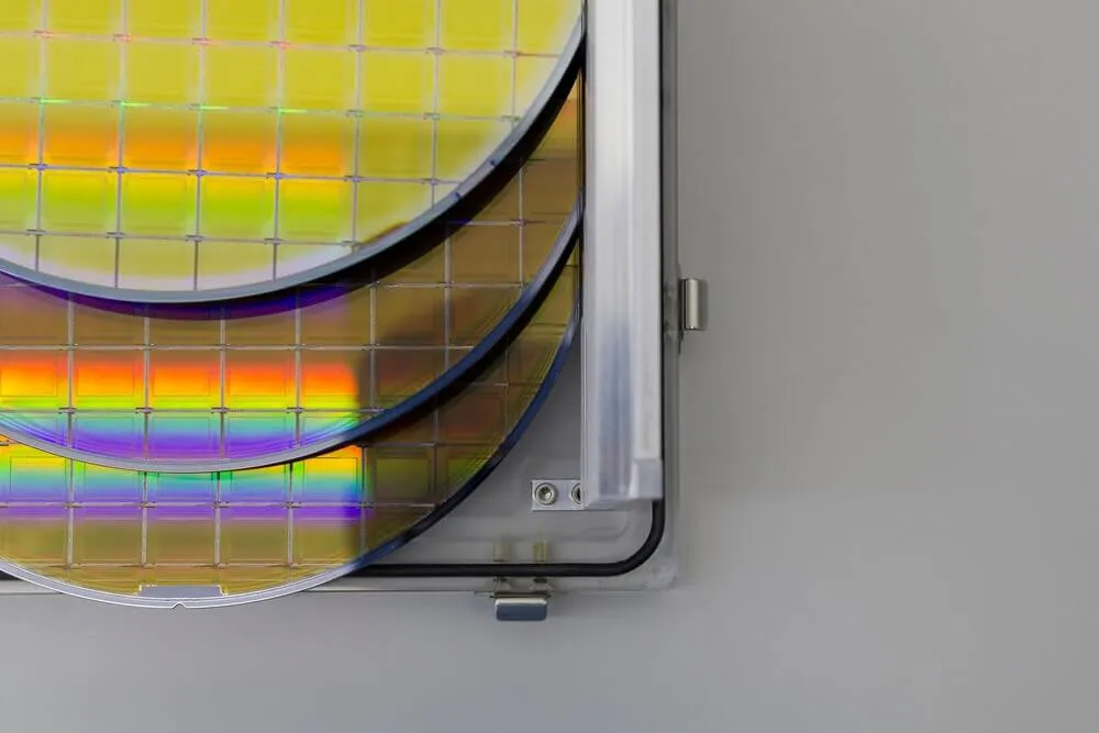
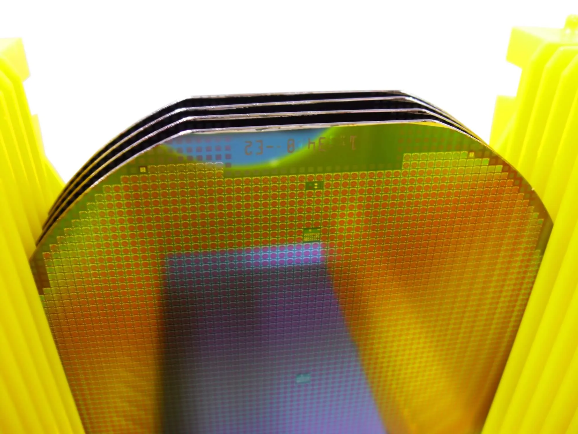
The grown silicon crystal is then sliced into thin circular wafers using a diamond saw. The thickness of these wafers can vary depending on the intended application, typically ranging from a few hundred micrometers to less than one millimeter.
The sliced wafers undergo a series of cleaning steps to remove impurities and contaminants from their surfaces. Chemicals and etchants are used to strip away any residual particles, oxides, or organic materials, ensuring a pristine surface for subsequent processing.
To impart specific electrical properties, dopant atoms are introduced into the silicon wafers through a process called diffusion or ion implantation. This step enables the creation of p-n junctions, critical for transistors, diodes, and other semiconductor devices.
By subjecting the wafers to high temperatures in an oxygen-rich environment, a thin layer of silicon dioxide is grown on their surfaces. This oxide layer acts as an insulator and protective coating, enabling further device integration and reducing surface defects.
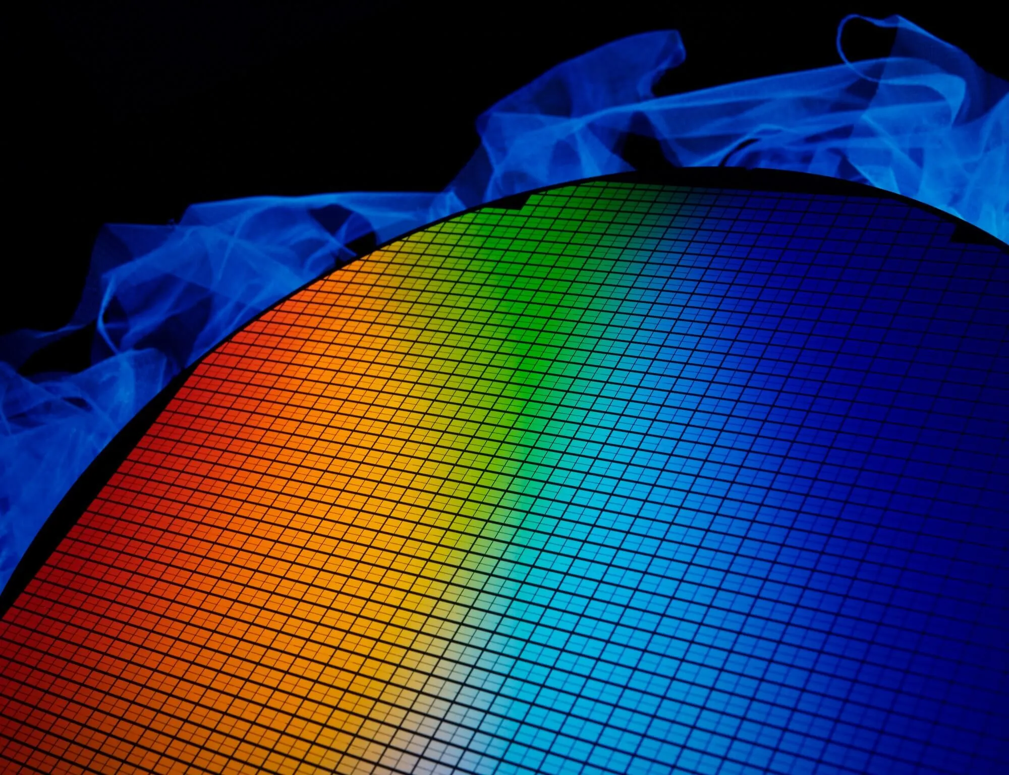
Photolithography involves transferring a pattern onto the wafer's surface using light-sensitive materials and masks. This pattern serves as a guide for subsequent etching processes, where specific areas of the oxide layer are selectively removed to expose the underlying silicon.
The silicon wafer-baking process is a complex and highly controlled series of steps, each contributing to the creation of high-quality silicon wafers. From crystal growth to surface preparation, dopant introduction, oxidation, and photolithography, every stage plays an important role in achieving the desired electrical properties and functionality of the final semiconductor devices.
With Wafer World, you will easily understand this process and gain a deeper appreciation for the intricate engineering behind the technology that powers our modern world. Call us to find out more!


