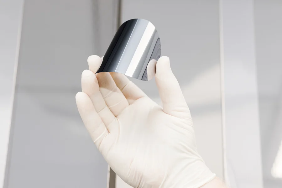
InP is valued for applications ranging from high-speed communications to photonic devices, but the substrate beneath those technologies has its own quality requirements. The crystal structure of an InP wafer can influence how successfully subsequent layers are grown and how consistently fabricated devices behave. Dislocations, strain, and other crystallographic irregularities are therefore more than material details. They can become practical concerns during device fabrication.
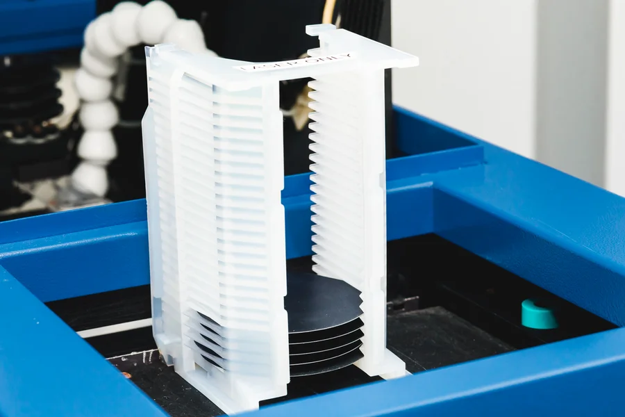
Dislocations are defects in the orderly arrangement of atoms within a crystal. Research indexed by the U.S. Department of Energy’s Office of Scientific and Technical Information notes that the properties of electronic and optoelectronic devices produced on InP substrates can be strongly affected by crystallographic defects, particularly dislocations.
Dislocations can originate during crystal growth. Research on vertical-gradient freeze growth has linked its generation to thermal stress within the growing crystal. Factors such as temperature gradients, crystal dimensions, growth direction, and growth rate can influence the conditions under which these defects form.
That relationship makes crystal quality partly a growth-control issue rather than something that can be addressed only after the ingot has been produced.
Many InP-based devices rely on epitaxy, in which additional semiconductor layers are deposited on a crystalline substrate. The quality of the starting crystal matters because the substrate provides the structural foundation for those layers.
NIST research has documented how defects in semiconductor substrates can interact with epitaxially layered systems. Some defects may propagate from the underlying substrate into deposited layers, while processing itself can introduce additional defects.
Crystal characteristics that may deserve attention include:
These factors should be considered together rather than assuming that a visually smooth surface confirms high crystal quality.
Uniformity is another important part of substrate evaluation. NIST characterization work on InGaAsP grown on InP has demonstrated that specimen nonuniformity can affect X-ray and photoluminescence measurements. Such characterization methods help researchers examine variations that may not be apparent through visual inspection alone.
Techniques such as X-ray diffraction provide a way to evaluate the crystal structure of semiconductors without relying solely on surface appearance. NASA has developed a non-destructive X-ray diffraction method for detecting crystal defects in cubic semiconductor wafers, including InP.
This distinction matters because polishing quality and crystal quality describe different aspects of a substrate. A surface can appear well finished while crystallographic imperfections remain within the material.
There is no universal crystal-quality specification for every InP-based device. Photonic components, high-frequency electronics, research structures, and other applications can place different demands on the substrate.
A useful purchasing approach is to define the device or research objective first, then review relevant substrate characteristics. Orientation, doping, electrical properties, dimensions, surface finish, and available crystal-quality information can all help determine whether a particular substrate is appropriate.
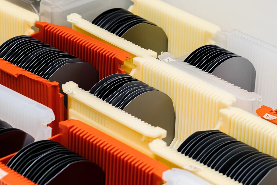
Selecting an InP wafer is easier when crystal characteristics are considered alongside the project's electrical, dimensional, and surface requirements. Wafer World can help you review available specifications and discuss substrate options based on your intended application. Contact us to schedule a consultation or call to discuss the material requirements for your next device, research program, or fabrication project.




