
When discussing semiconductor materials, the terms silicon manufacturing and wafer fabrication are often used interchangeably, but they refer to distinct stages in the production process. Understanding the difference between these two is essential for anyone involved in electronics, engineering, or material sourcing. Each step plays a unique role in transforming raw silicon into a usable form for advanced technologies, and recognizing how they connect helps ensure better decision-making and improved results.
Silicon manufacturing is the foundational stage where raw silicon is extracted, purified, and prepared for further processing. This phase begins with silicon dioxide, commonly found in sand, which undergoes a series of chemical and thermal processes to produce high-purity silicon. The goal is to achieve a level of purity suitable for semiconductor applications, often reaching extremely low impurity concentrations. This stage is critical because the quality of the starting material directly impacts the performance of the final product.
The process involves refining silicon through methods such as chemical vapor deposition and zone refining. These techniques help remove impurities and create uniform crystal structures. The result is a material that meets strict industry requirements for electronic applications. Consistency during this stage ensures that the silicon behaves predictably in later processes, supporting reliable performance across a wide range of uses.
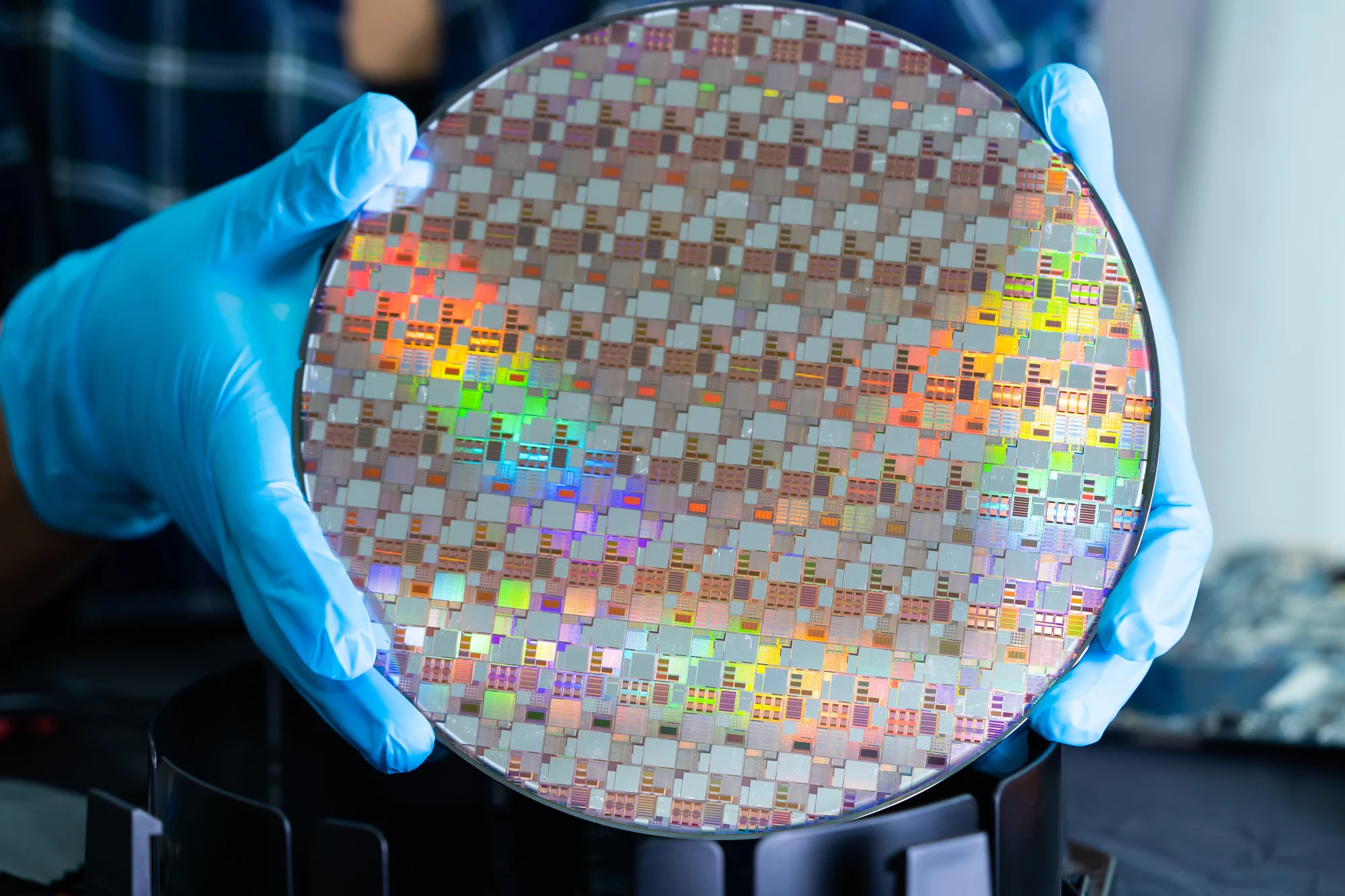
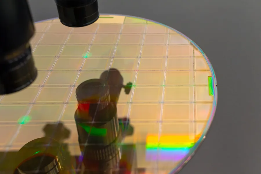
Wafer fabrication focuses on shaping purified silicon into thin, uniform wafers for device production. This stage transforms bulk silicon into a format that supports precise engineering and integration into electronic systems. The process includes slicing, polishing, and preparing the wafer surface to meet exact specifications.
Wafers must meet strict standards for thickness, flatness, and surface quality. Advanced polishing techniques are used to create smooth surfaces that support accurate patterning during device fabrication. This precision is essential for ensuring that electronic components function as intended. Without proper wafer preparation, even high-quality silicon cannot deliver consistent results.
The primary difference between these two stages lies in their scope and objectives. Silicon manufacturing concerns the creation of the raw material, while wafer fabrication focuses on shaping it into a usable form. Each stage requires different expertise, equipment, and quality controls.
Silicon manufacturing emphasizes chemical purity and crystal growth, ensuring that the material meets strict standards. Wafer fabrication, on the other hand, prioritizes physical precision and surface integrity. Both are essential, but they address different aspects of the production process. Understanding this distinction helps clarify where specific challenges and opportunities may arise.
Consistency is a critical factor in both silicon manufacturing and wafer fabrication. Variability in either stage can lead to defects or performance issues in the final product. Maintaining strict quality control ensures that materials meet required specifications at every step.
Uniformity supports predictable outcomes in semiconductor production. When materials are consistent, engineers can rely on stable processes and reduce the need for adjustments. This leads to improved efficiency and better overall performance. Long-term success in semiconductor manufacturing depends on maintaining this level of consistency.
Traceability plays an important role in ensuring quality and accountability. Both stages require detailed documentation to track material origins, processing conditions, and batch information. This transparency helps identify potential issues and supports continuous improvement.
Accurate records allow manufacturers to verify material history and maintain compliance with industry standards. When issues arise, traceability provides a clear path for investigation and resolution. This level of detail contributes to greater confidence in the final product.
Contamination control is essential throughout the production process. Even small amounts of impurities can affect material performance and reliability. Clean environments and strict handling procedures help protect silicon at every stage.
Maintaining controlled environments reduces the likelihood of defects and ensures that materials remain within specification. Consistent contamination control practices support both silicon manufacturing and wafer fabrication, helping preserve the integrity of the material.
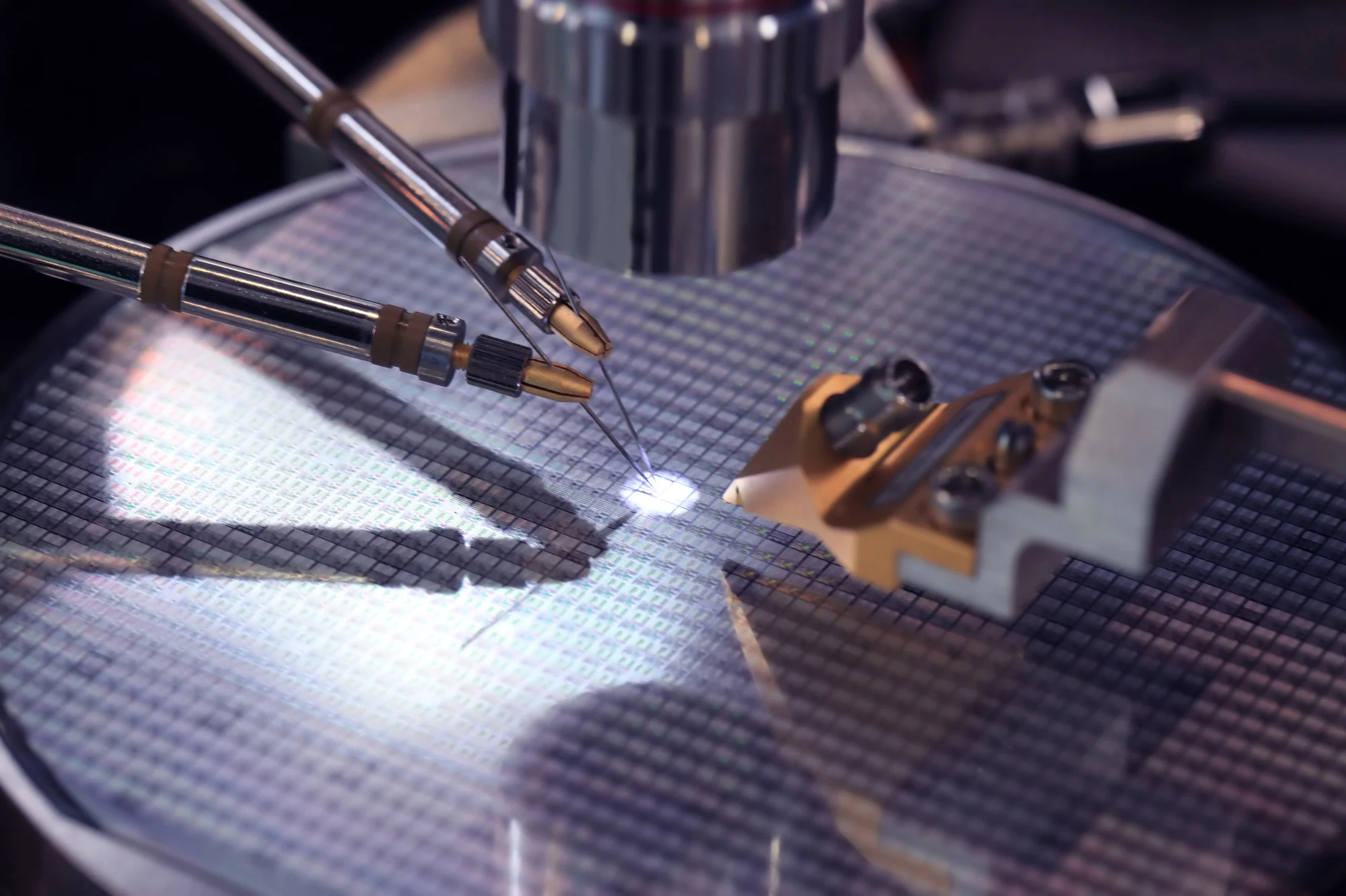
Inspection is used to confirm that materials meet required standards before moving to the next stage. Both silicon manufacturing and wafer fabrication rely on detailed inspection methods to assess quality and identify potential issues.
Consistent inspection protocols provide valuable data that supports decision-making and process optimization. By verifying material characteristics at each stage, manufacturers can maintain control over quality and reduce the risk of defects.
Proper packaging and handling are important for maintaining material quality during storage and transportation. Wafers, in particular, require careful handling to prevent damage or contamination.
Standardized packaging solutions help ensure that materials arrive in optimal condition. This supports efficient production and reduces the risk of delays caused by damaged or compromised materials. Attention to detail in this area contributes to overall reliability.
Efficient coordination between silicon manufacturing and wafer fabrication is essential for maintaining consistent lead times. Delays in either stage can impact production schedules and overall efficiency.
Clear communication and well-managed processes help ensure that materials are available when needed. Consistency in supply chain operations supports better planning and reduces uncertainty.
Silicon manufacturing and wafer fabrication are interconnected stages that work together to create high-quality semiconductor materials. While they serve different purposes, both are essential for achieving reliable performance and long-term success. Understanding how these processes differ and how they complement each other allows for more informed decisions and better outcomes in semiconductor production.
If you are looking to understand your material options better and improve production efficiency, working with the right partner can make a meaningful difference. Wafer World supports engineers and manufacturers with consistent materials and practical insights, helping you navigate silicon manufacturing with greater confidence and clarity. Connect with us today to schedule a consultation and take the next step toward more reliable and efficient semiconductor processes built on trusted silicon manufacturing practices.


