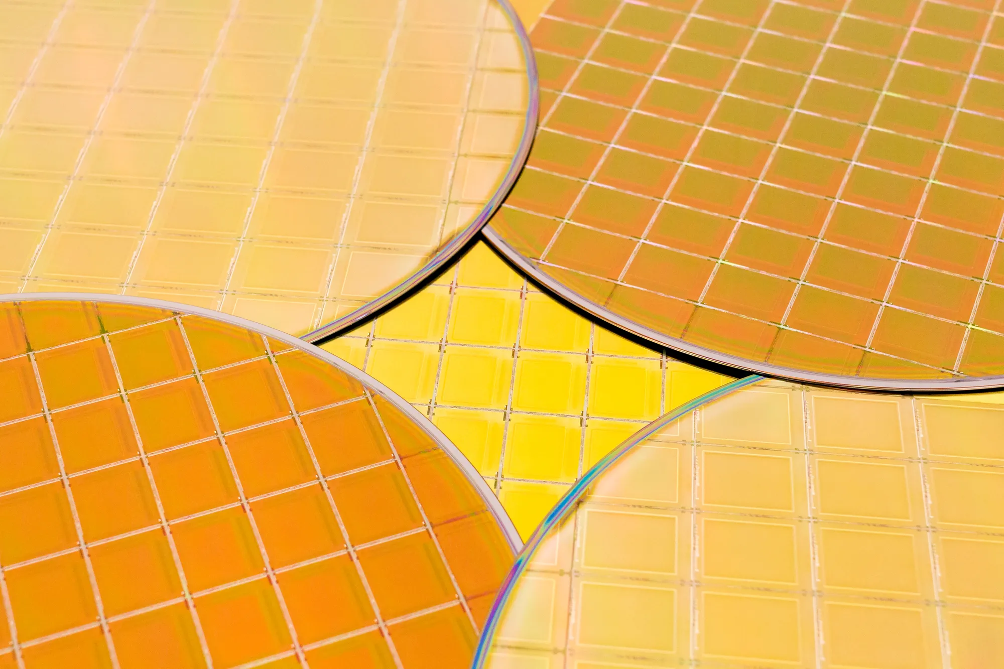
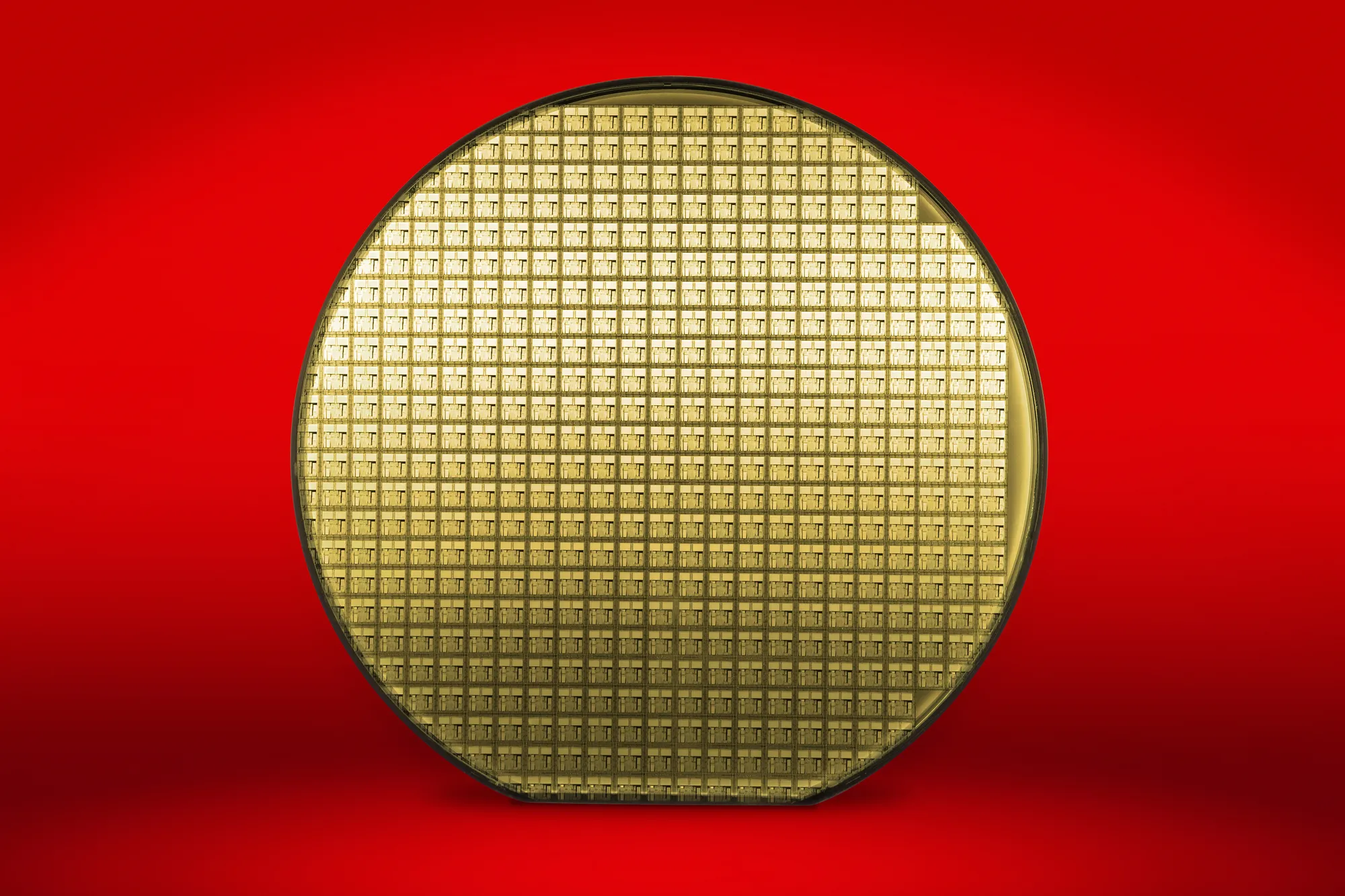
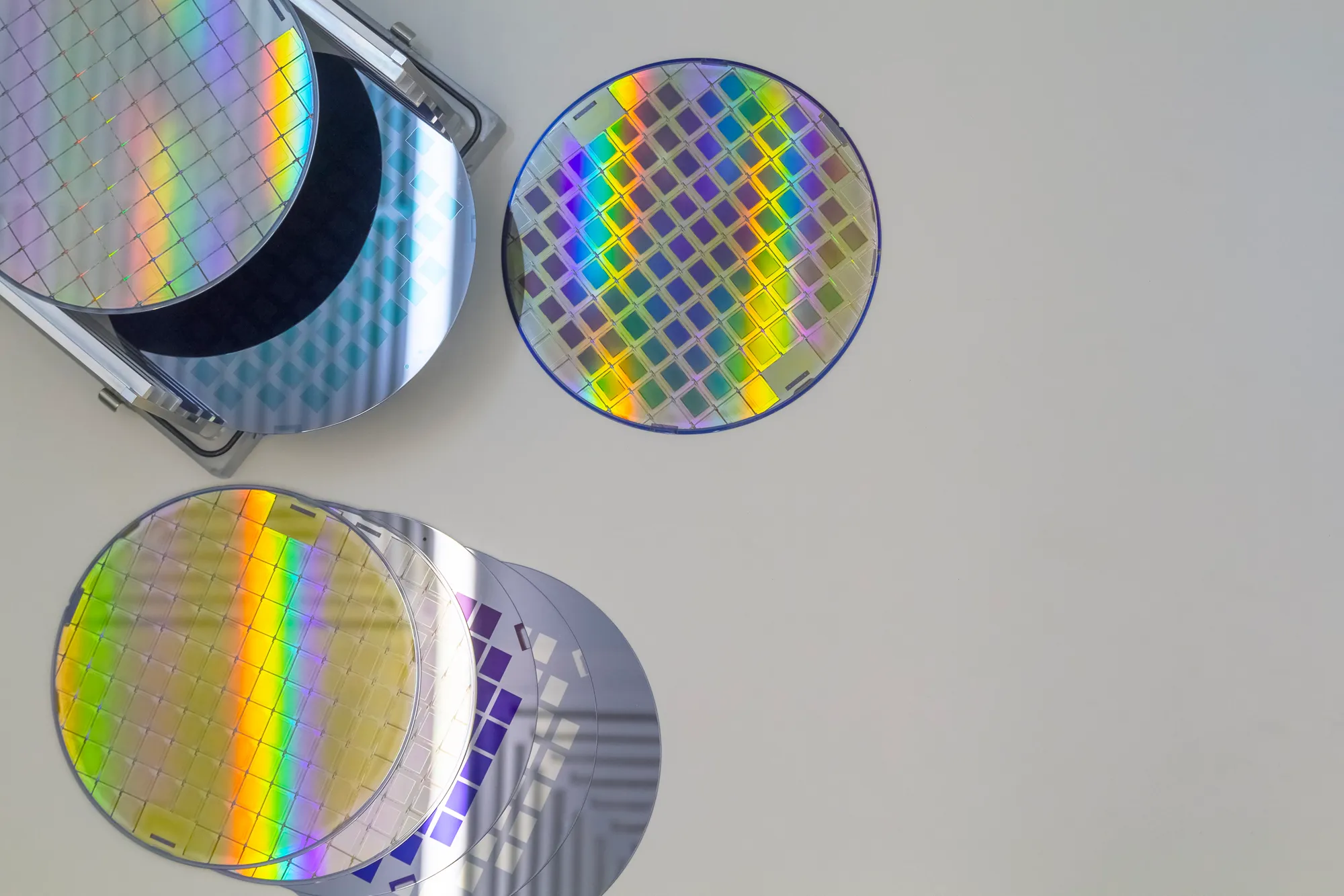
InP (Indium Phosphide) wafers have emerged as a crucial material in the realm of semiconductor technology, enabling the development of cutting-edge electronic devices and systems. With its exceptional electronic and optoelectronic properties, InP wafers have found numerous applications across various industries. In this blog post, we delve into and highlight the significance of powering next-generation InP wafer technologies.
InP wafers serve as the backbone of high-speed communication systems, including fiber-optic networks and telecommunications. InP-based optoelectronic devices, such as lasers, modulators, and photodetectors, offer superior performance in terms of bandwidth, speed, and efficiency. These components are pivotal in transmitting vast amounts of data over long distances with minimal signal degradation.
InP wafers have gained traction in the field of photovoltaics, offering a promising alternative to traditional silicon-based solar cells. The high electron mobility and superior absorption properties of InP make it an excellent material for efficient solar energy conversion.
InP-based solar cells have demonstrated impressive power conversion efficiencies, making them ideal for space applications and other scenarios where high performance is crucial.
InP wafers have revolutionized the realm of high-frequency electronics. The material's superior electron velocity and high breakdown voltage enable the fabrication of high-performance transistors, amplifiers, and other electronic components operating at microwave and millimeter-wave frequencies. These advancements pave the way for the development of advanced radar systems, wireless communication networks, and satellite communication devices.
InP wafers play a pivotal role in the burgeoning field of quantum technologies. Researchers harness the unique quantum properties of InP to create devices such as single-photon sources and quantum dots. These advancements are vital in realizing quantum cryptography, quantum computing, and quantum communication systems, which hold immense potential for transforming information processing and encryption.
InP wafers have become indispensable in driving technological advancements across various sectors. From high-speed communication and photovoltaics to high-frequency electronics and quantum technologies, the remarkable properties of InP enable the development of next-generation devices and systems.
As research and innovation continue to unlock the full potential of InP, Wafer World can anticipate even more groundbreaking applications that will shape the future of technology. Call us now for more details!


