August 21, 2023
Shop NowIn the field of semiconductor manufacturing, reliability and precision are extremely important. The demand for increasingly sophisticated microchips has led to the widespread adoption of laser-based techniques for marking, etching, and engraving on wafers. These processes play pivotal roles in ensuring the quality, functionality, and traceability of integrated circuits. However, understanding the differences between laser marking, laser etching, and engraving is crucial for making informed decisions in this fast-evolving industry.
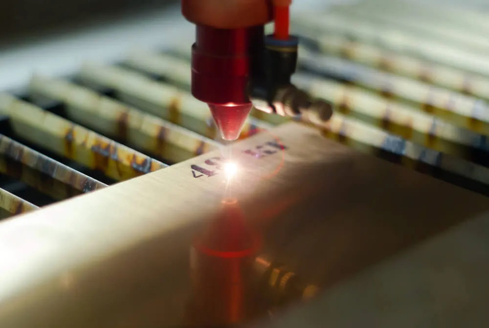
Laser marking is a non-contact process that modifies the surface of a wafer by inducing a color change through chemical or physical reactions. The laser beam interacts with the material, creating high-contrast marks without affecting the substrate's integrity.
It is primarily used for labeling and identification purposes, such as adding QR codes, serial numbers, or logos on wafers. The process is rapid, precise, and provides high legibility, ensuring seamless traceability throughout the production chain.
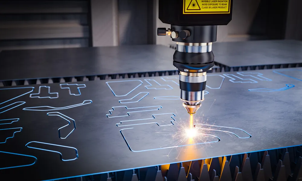
Laser etching is a subtractive process wherein the laser beam vaporizes specific areas of the wafer's surface to create shallow indentations or cavities. This controlled material removal allows for the creation of intricate designs or patterns, often used for aesthetic or functional purposes in microelectronics. The depth of the etched features can be precisely controlled, making it suitable for fine structures like microfluidic channels or MEMS (Micro-Electro-Mechanical Systems).
Laser engraving, on the other hand, is a more profound and more permanent process compared to laser etching. The laser beam removes material in a way that leaves a visible depression on the wafer's surface. Engraving is often utilized for decorative purposes, logos, and branding. While it provides a lasting mark, the depth involved might have implications for the wafer's structural integrity, making it less common in semiconductor production.
Choosing the appropriate laser-based process for wafers depends on the specific application requirements. For instance, laser marking is ideal for batch identification and tracking, while laser etching is preferred for creating microstructures. Engraving may be suitable for decorative elements, but careful consideration of its impact on wafer performance is necessary.
Laser marking, laser etching, and engraving offer unique capabilities to the semiconductor industry. Each technique brings value in its distinct way, enhancing efficiency, functionality, and aesthetics for microelectronics. Wafer World grasps the subtleties of these processes to make informed decisions and push the boundaries of semiconductor technology further. Call us today!


