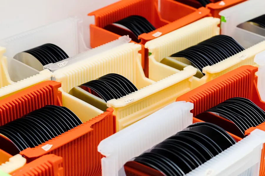
"Wafer World has completed the acquisition of, MRT, Micro Reclaim Technologies as of January 1st 2026"
What’s driving silicon prices in 2026? Understand market trends and factors affecting silicon costs in the electronics industry.
Read MoreThin silicon wafers are driving innovation in electronics. Discover their role in enhancing performance and compact device design.
Read More
Silicon wafer processing is evolving rapidly. Find out how recent innovations are reshaping the electronics industry for better performance and reliability.
Read More
Explore the science behind InP wafers and their role in modern applications like 5G, sensing, and high-frequency semiconductor devices.
Read MoreLearn about the materials involved in silicon wafer manufacturing and how they impact the efficiency and reliability of semiconductor devices.
Read MoreExplore the cutting-edge technologies used by silicon wafer manufacturers to improve efficiency in production, reducing waste and enhancing performance.
Read More
InP reclaim wafers help reduce costs, improve efficiency, and support sustainable compound semiconductor manufacturing processes.
Read More
Here’s how GaAs wafers contribute to enhanced semiconductor device performance, offering faster processing speeds and improved efficiency.
Read More
FZ wafers benefit engineers and buyers seeking high-purity materials for advanced semiconductor designs.
Read More