.webp)
Stay up-to-date with the latest news and trends in wafer and semiconductor technologies.
*Blogs are for educational and informational purposes ONLY
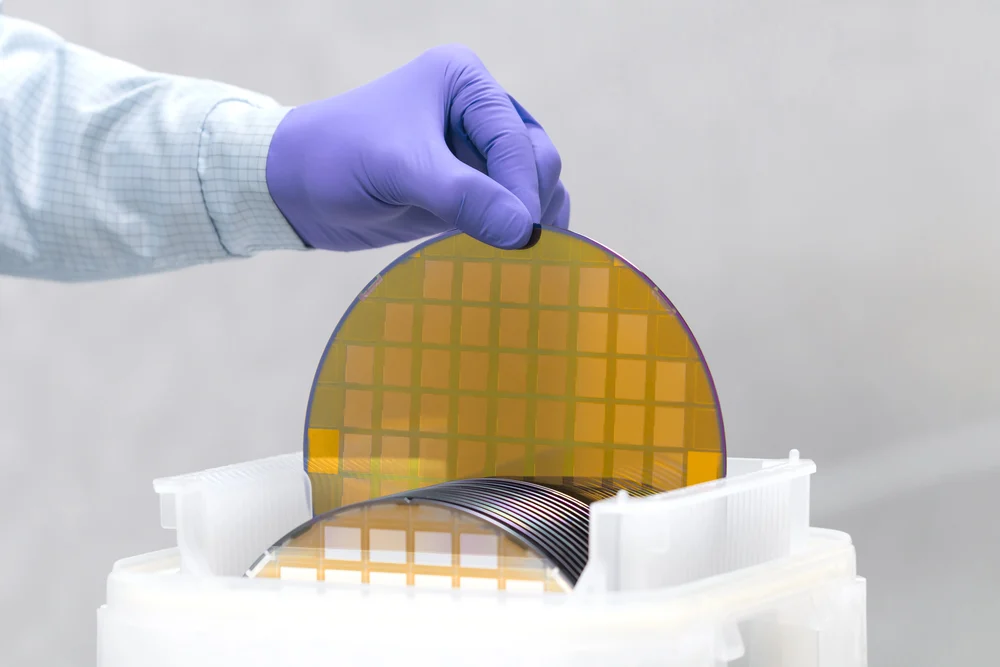
Understand how modern silicon wafer manufacturing integrates sustainability, quality control, and long-term supply reliability.
Read More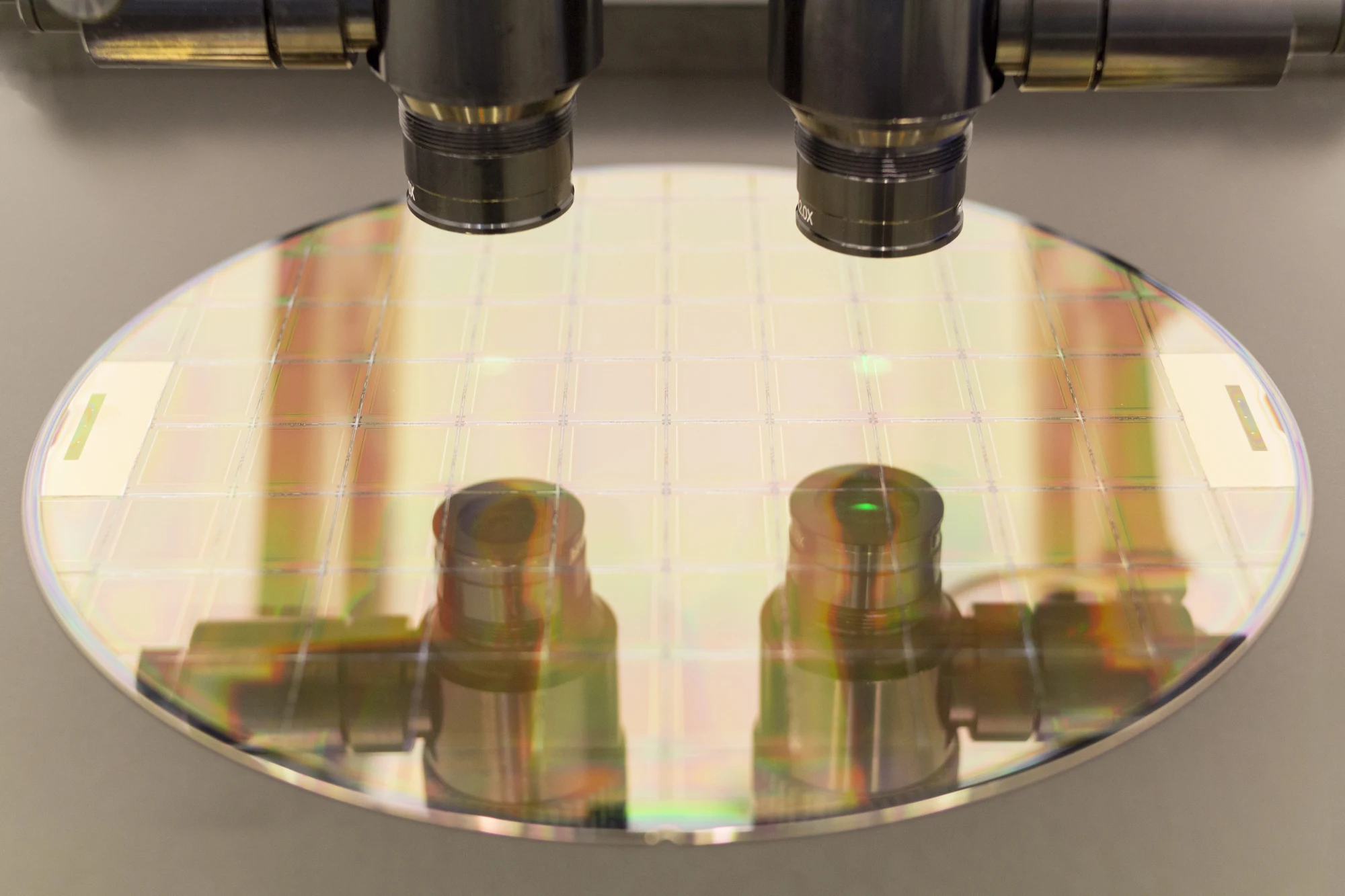
A closer look at silicon manufacturing for modern power devices & ICs, covering crystal growth, wafer prep, and application-driven specs.
Read More
Learn how FZ wafer compares to CZ wafers in resistivity, defect control, and reliability for advanced semiconductor devices.
Read More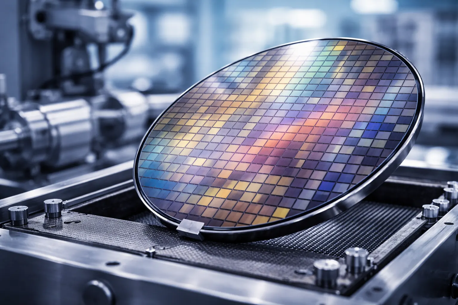
A practical guide to Si wafer diameter, orientation, and resistivity to help engineers select the right substrate for device performance.
Read More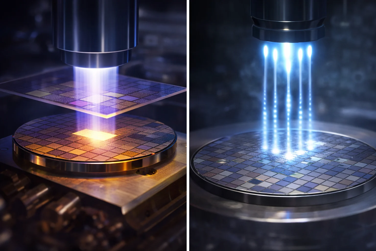
A clear overview of silicon wafer processing methods, including oxidation, doping, lithography, and etching in semiconductor fabrication.
Read More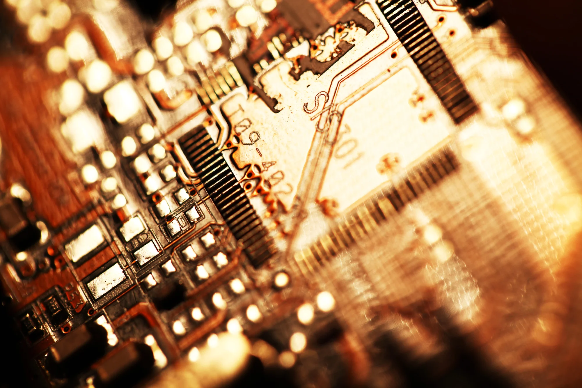
Explore the factors influencing silicon prices in today’s semiconductor market, from raw materials to global demand and supply chain shifts.
Read More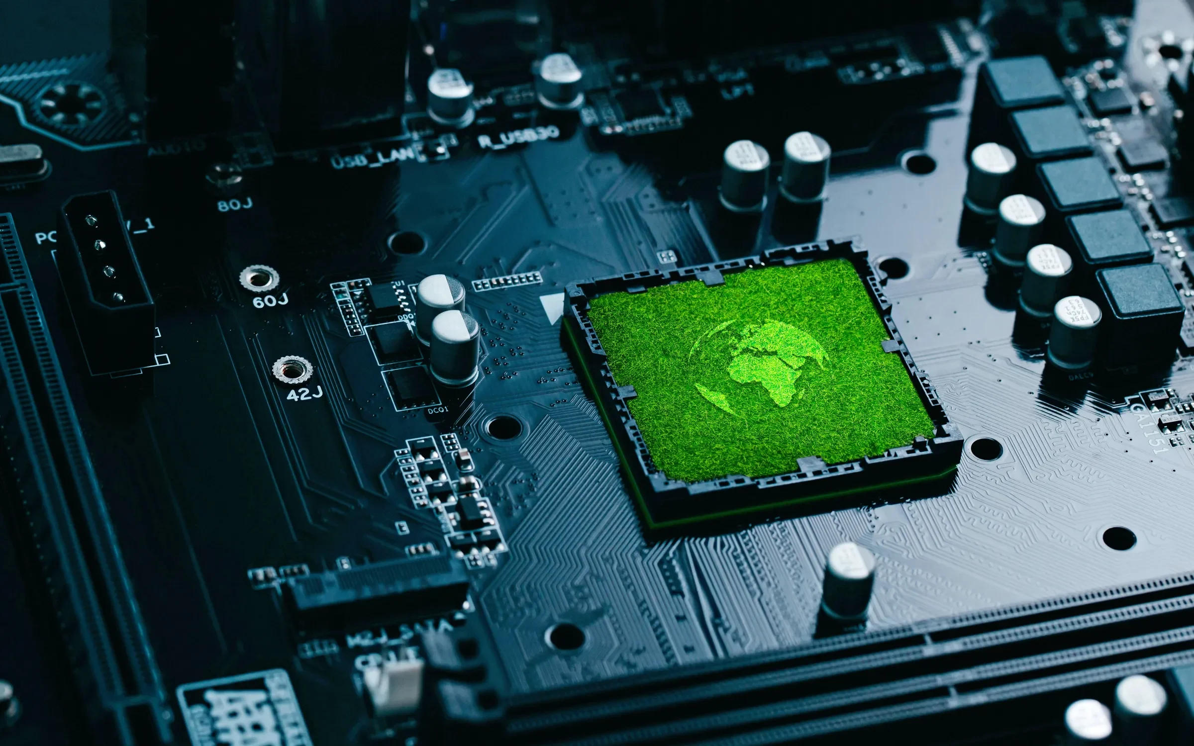
A practical guide to choosing silicon wafer manufacturers that meet strict OEM standards for quality and technical performance.
Read More
InP wafer technology is advancing rapidly. Discover the latest trends, challenges, and prospects of this essential component in semiconductor applications.
Read More
Discover how ultra flat wafers enhance MEMS sensitivity and power device efficiency through superior planarity, uniformity, and process stability.
Read More
Learn why GaAs wafer substrates are essential for RF amplifiers, microwave circuits, and next-generation 5G applications.
Read More