.webp)
Stay up-to-date with the latest news and trends in wafer and semiconductor technologies.
*Blogs are for educational and informational purposes ONLY

Confused about SI wafers vs. fused silica wafers? Learn the key material differences, applications, and how to choose the right wafer for your process.
Read More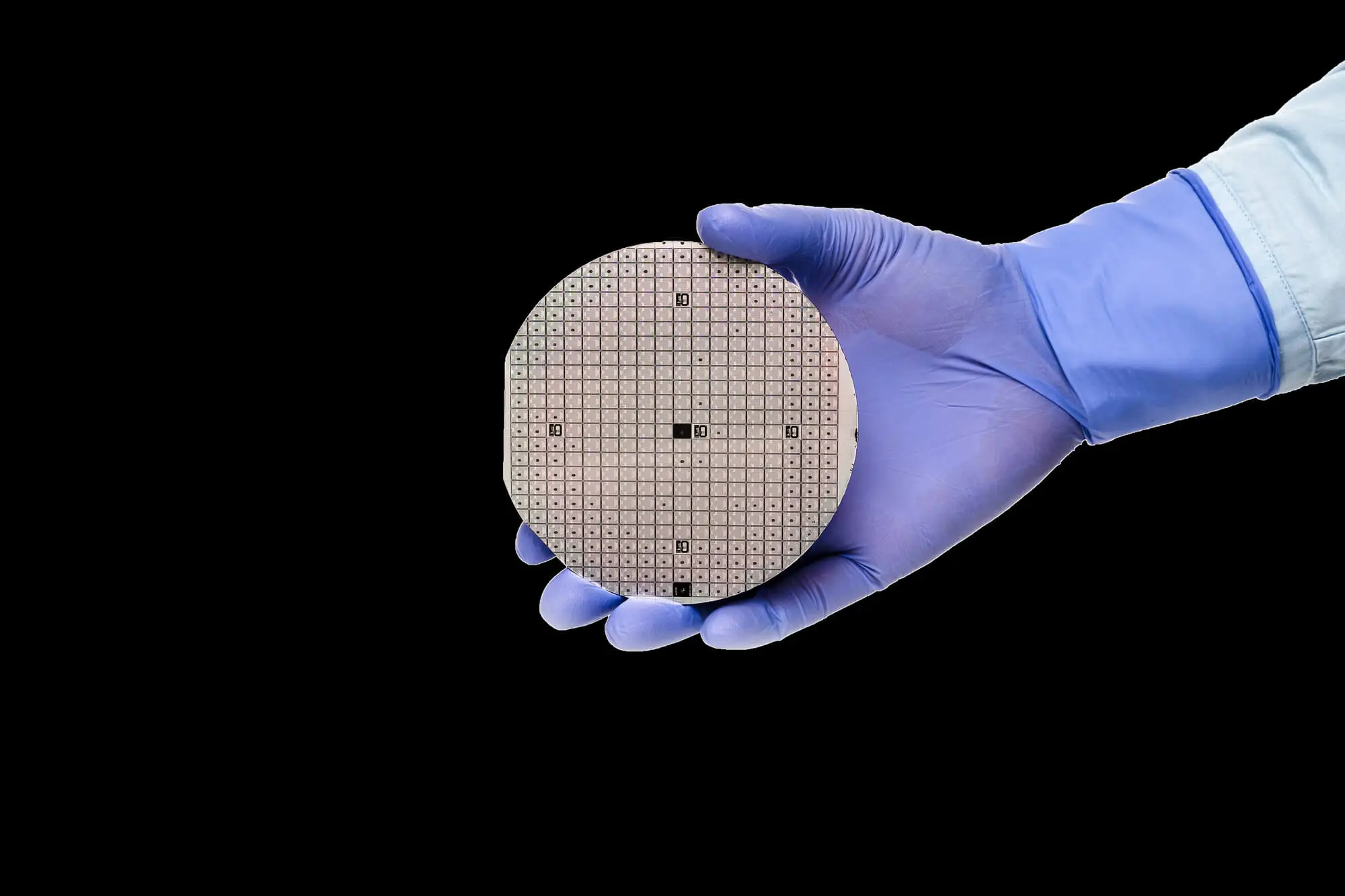
Learn what SOI wafers are, how they work, and when to buy silicon wafers with SOI for RF, power, and advanced CMOS devices.
Read More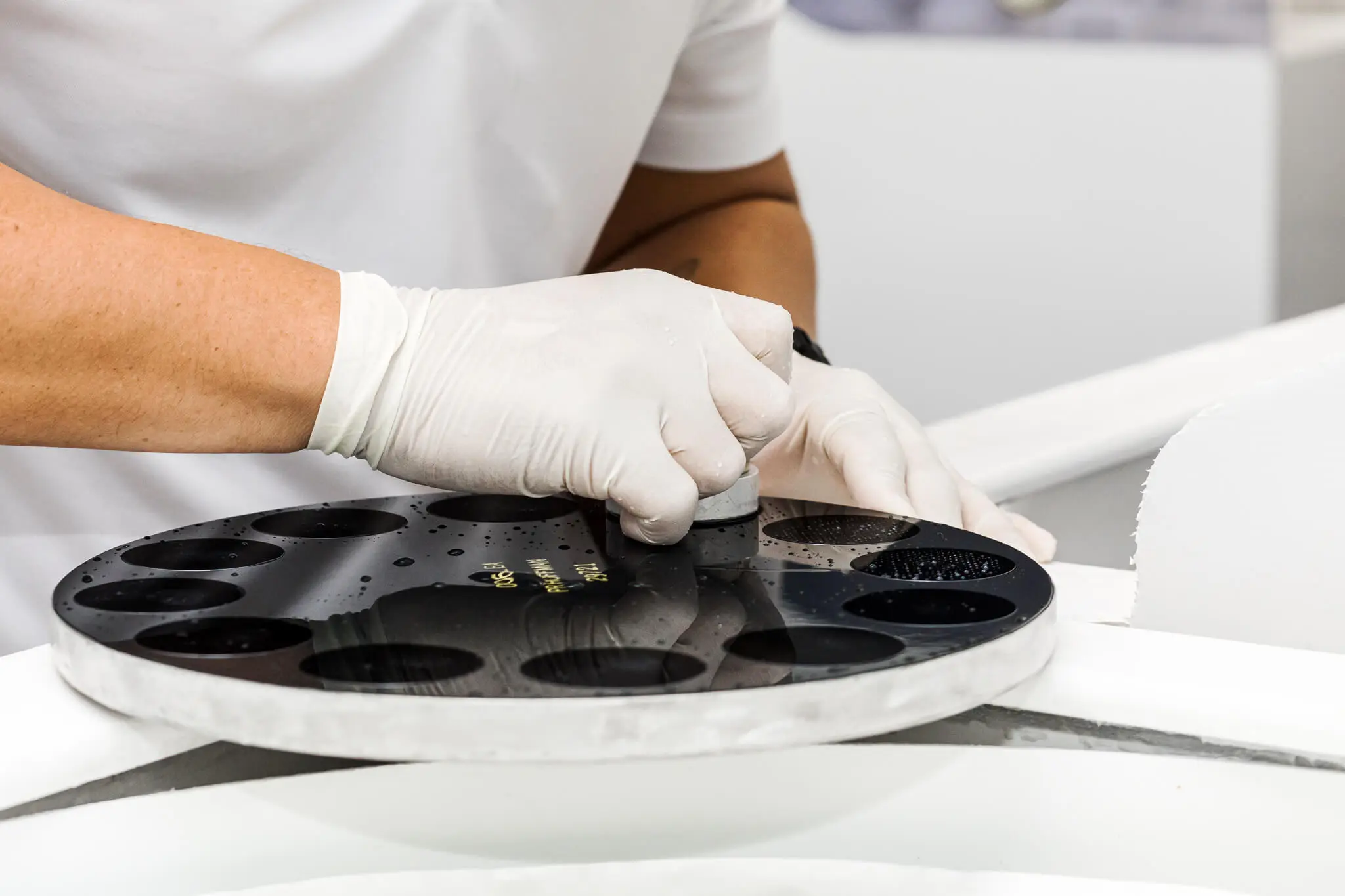
Discover how CPUs and computer chips are made step by step—and why double side polish wafers are critical for precision and yield.
Read More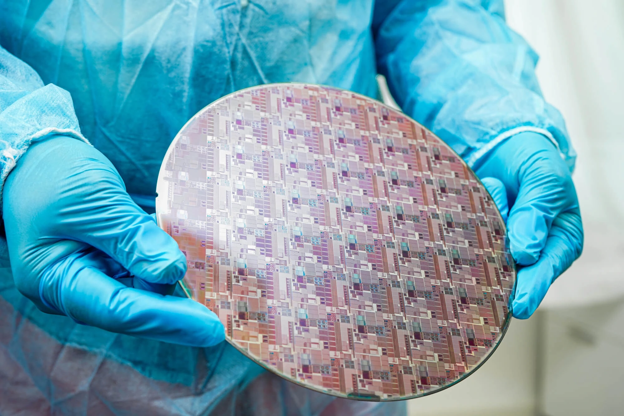
Learn what SiO₂ wafers are, how they’re used in semiconductor manufacturing, and what to consider when you buy silicon wafers for your application.
Read More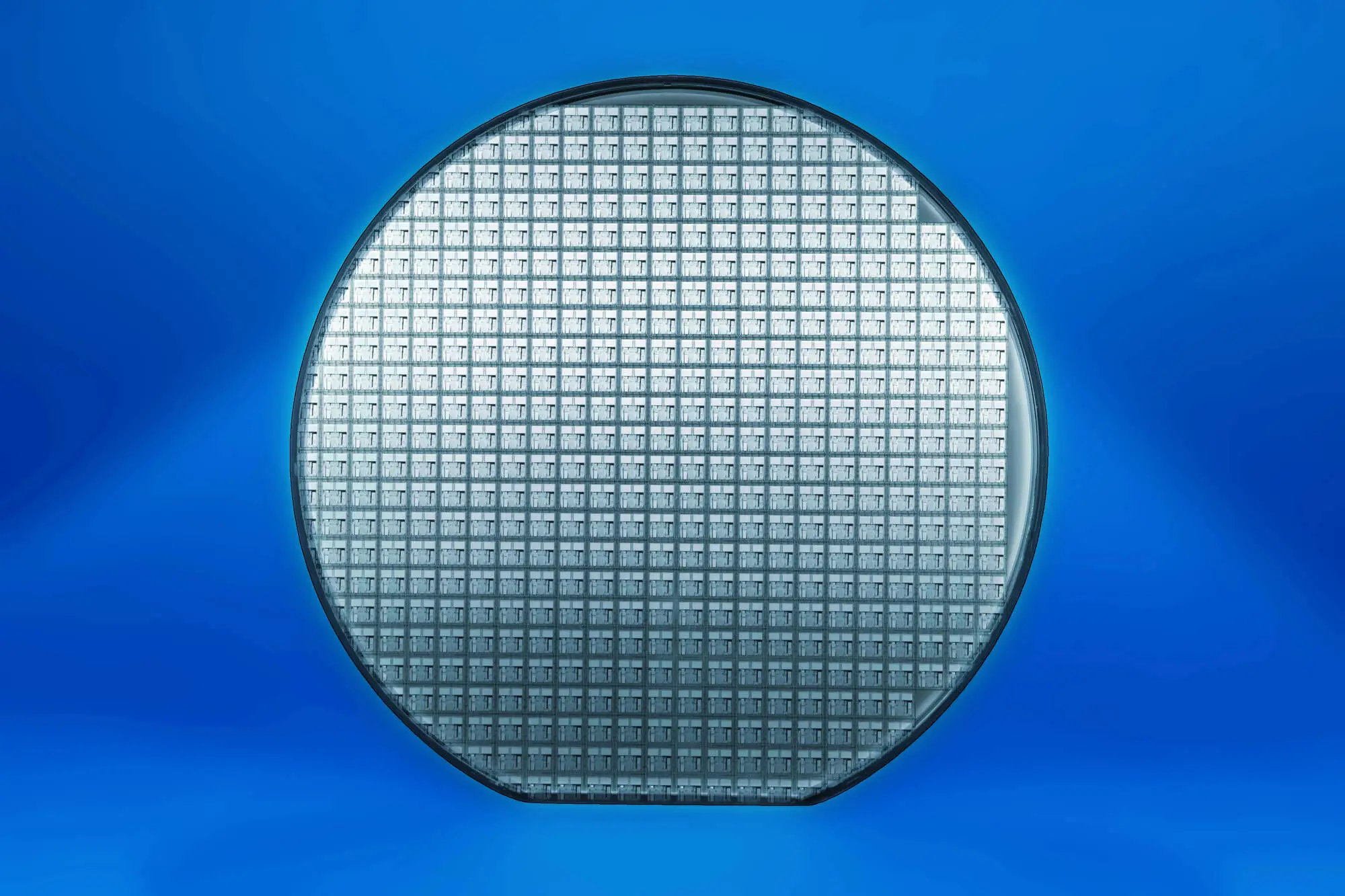
Learn when thin silicon wafers require epitaxial layers, how epi wafers are made, and why they improve device performance and yield.
Read More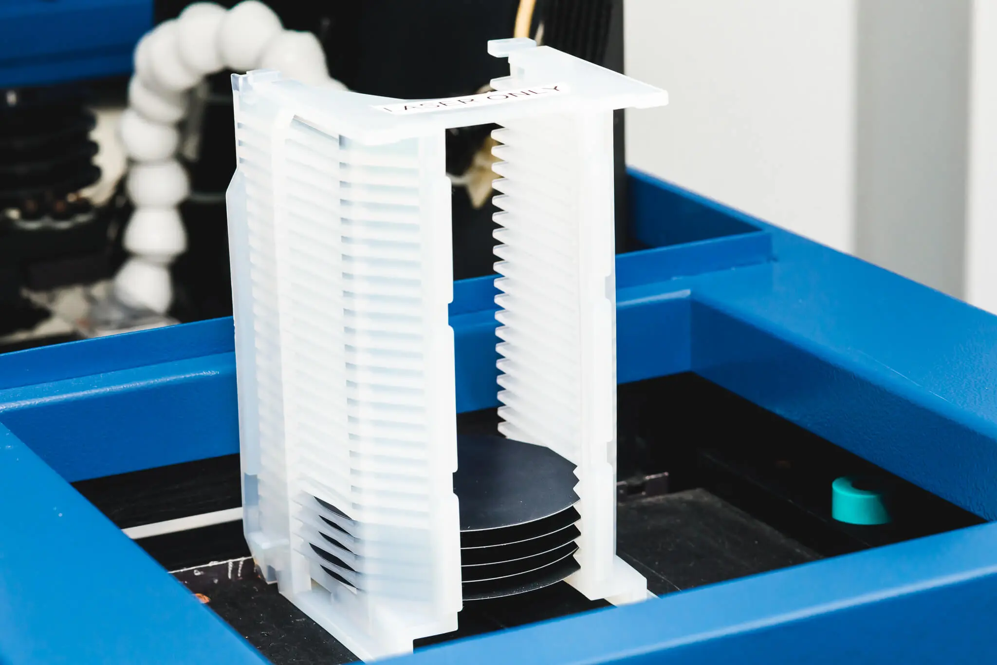
Laser marking is critical for InP reclaim wafers. Learn recommended methods to avoid defects, ensure compliance, and improve wafer traceability.
Read More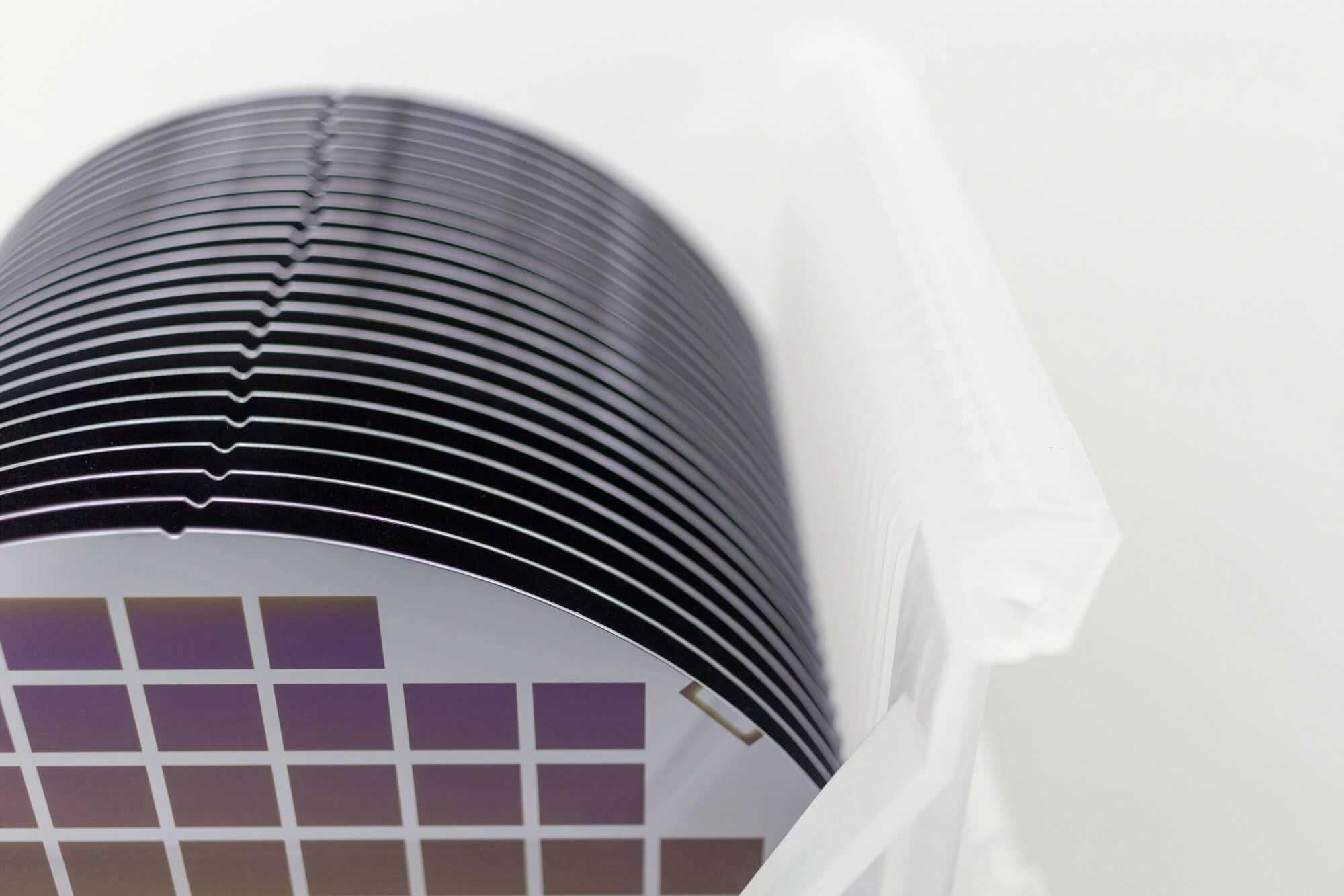
Discover how many dies a germanium wafer can produce based on wafer size, die layout, and yield. Learn what impacts cost and efficiency before sourcing!
Read More
Curious about silicon nitride wafers? Learn how they’re used in semiconductors, their limitations, and when silicon wafer suppliers recommend them.
Read More
Explore the 2025 InP wafer market—current prices, supply trends, demand forecasts, and key factors to make smarter purchasing decisions and secure reliable suppliers.
Read More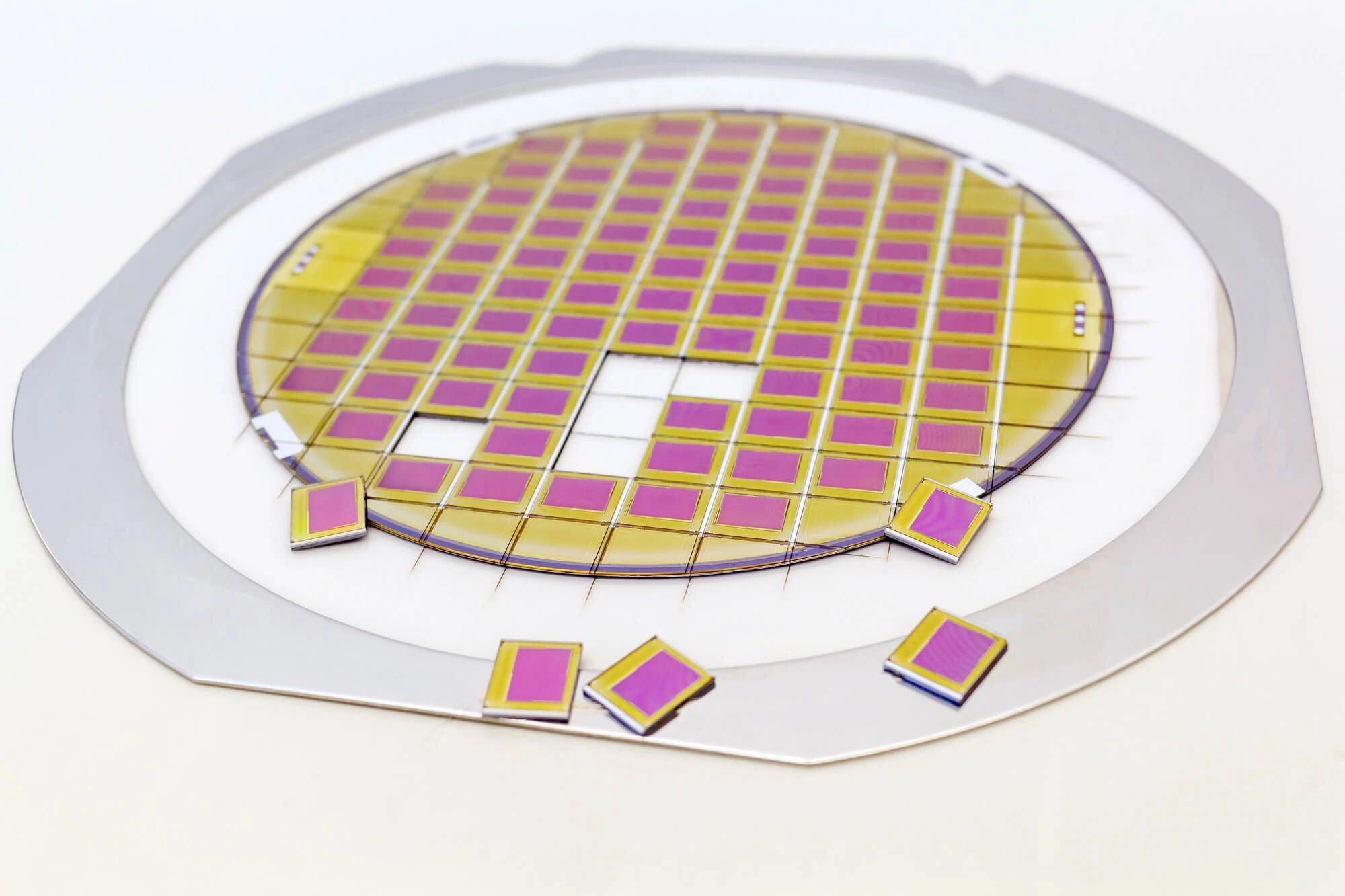
Learn how silicon lattice constant and crystal orientation impact wafer manufacturing—boosting device yield, performance, and design precision.
Read More