.webp)
Stay up-to-date with the latest news and trends in wafer and semiconductor technologies.
*Blogs are for educational and informational purposes ONLY
Silicon carbide is an important material in wafer manufacturing. But what are the advantages and uses of this material, and what makes it different from silicon?
Read More
When looking for the right silicon wafer for your project, crystal orientation is a key factor to consider. But how does this affect semiconductors?
Read More
Depending on your project, your silicon wafer supplier may suggest an epitaxial growth wafer over standard silicon. But how do these two options compare?
Read More
Besides silicon, a germanium wafer can also be used when manufacturing solar cells. But what are the benefits—and disadvantages—of this material?
Read More
Understanding how a float zone wafer reacts to THz radiation is essential for optimizing THz optics and detection devices.
Read More.webp)
Most silicon wafer suppliers also handle other materials, such as sapphire. Learn here the uses of sapphire wafers and how reclaimed ones can help you cut costs.
Read More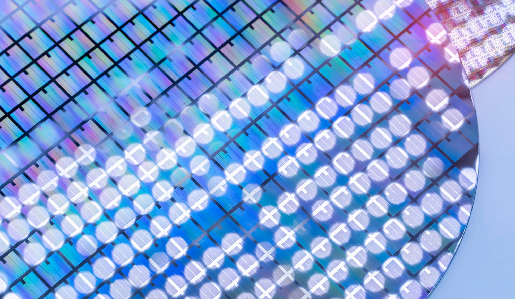
A double side polish wafer offers several benefits, from high precision to enhanced flatness—but when are these advantages unnecessary?
Read More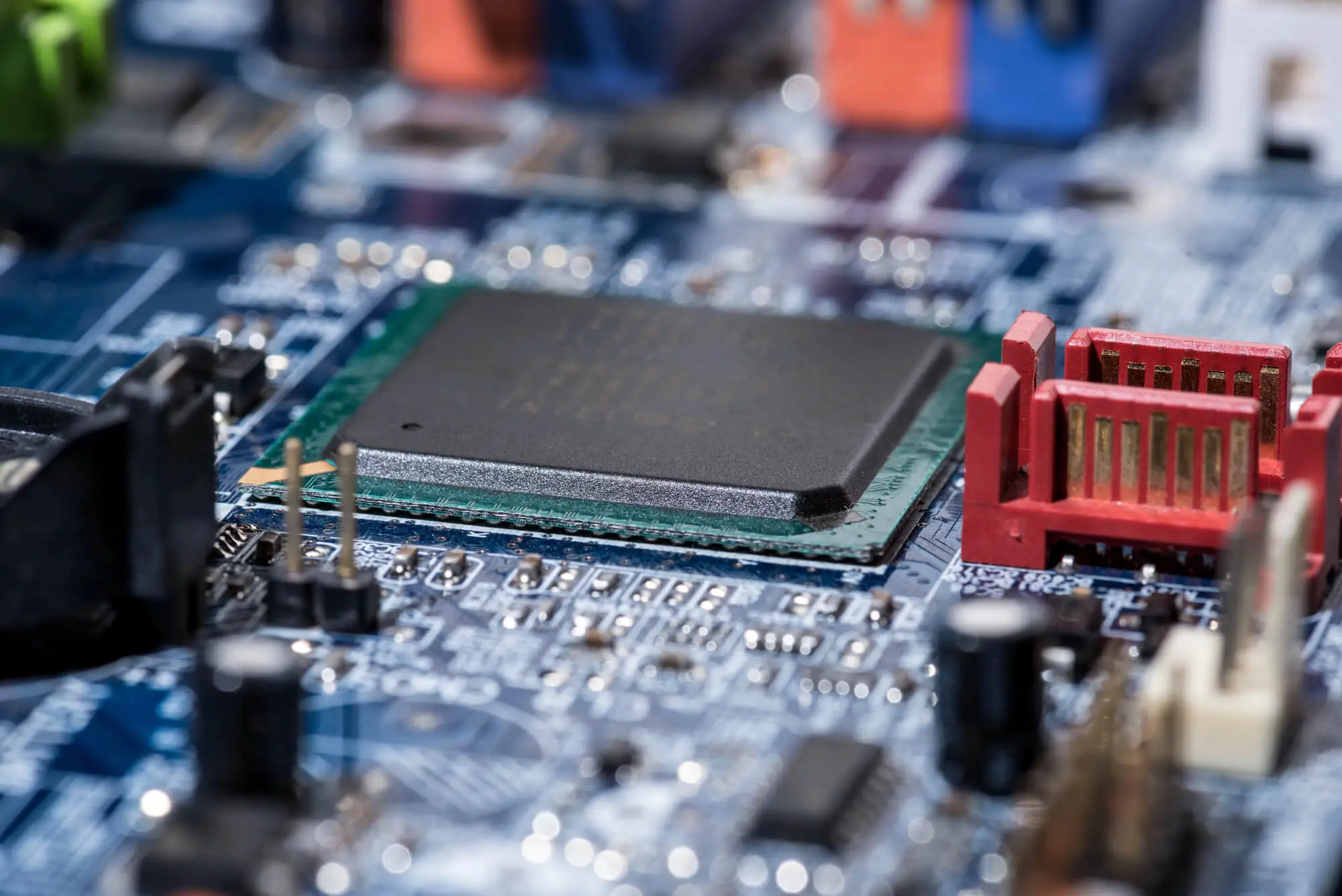
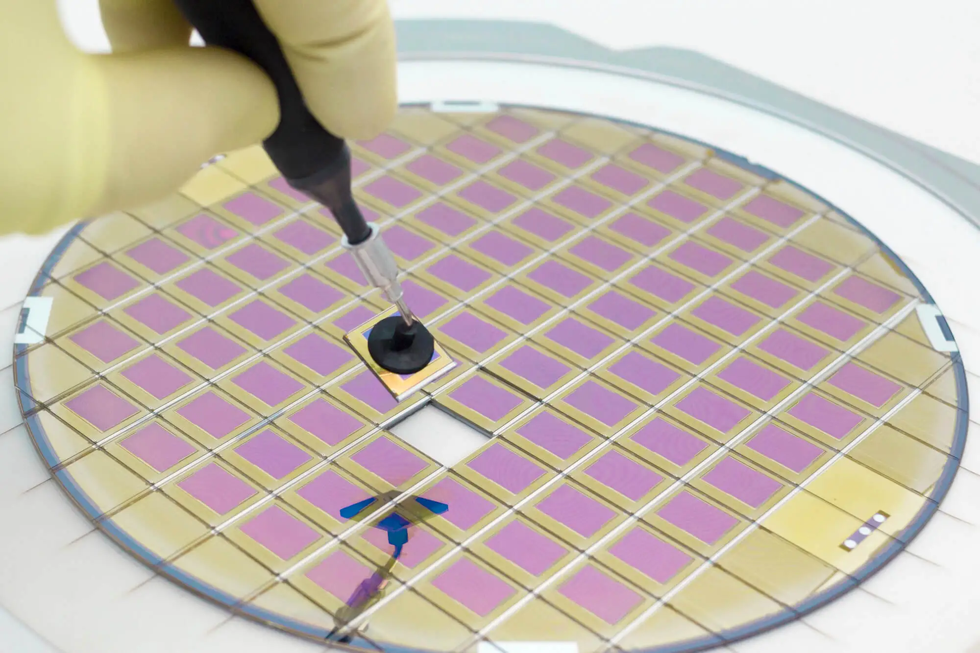
Bonding substrates from silicon wafer suppliers can produce more effective, durable, and comprehensive chips. Here are some bonding techniques worth knowing about.
Read More
Behind the spurt of more realistic AI generators lies the growth in wafer manufacturing. Here, we’ll explain the role of wafers in AI images.
Read More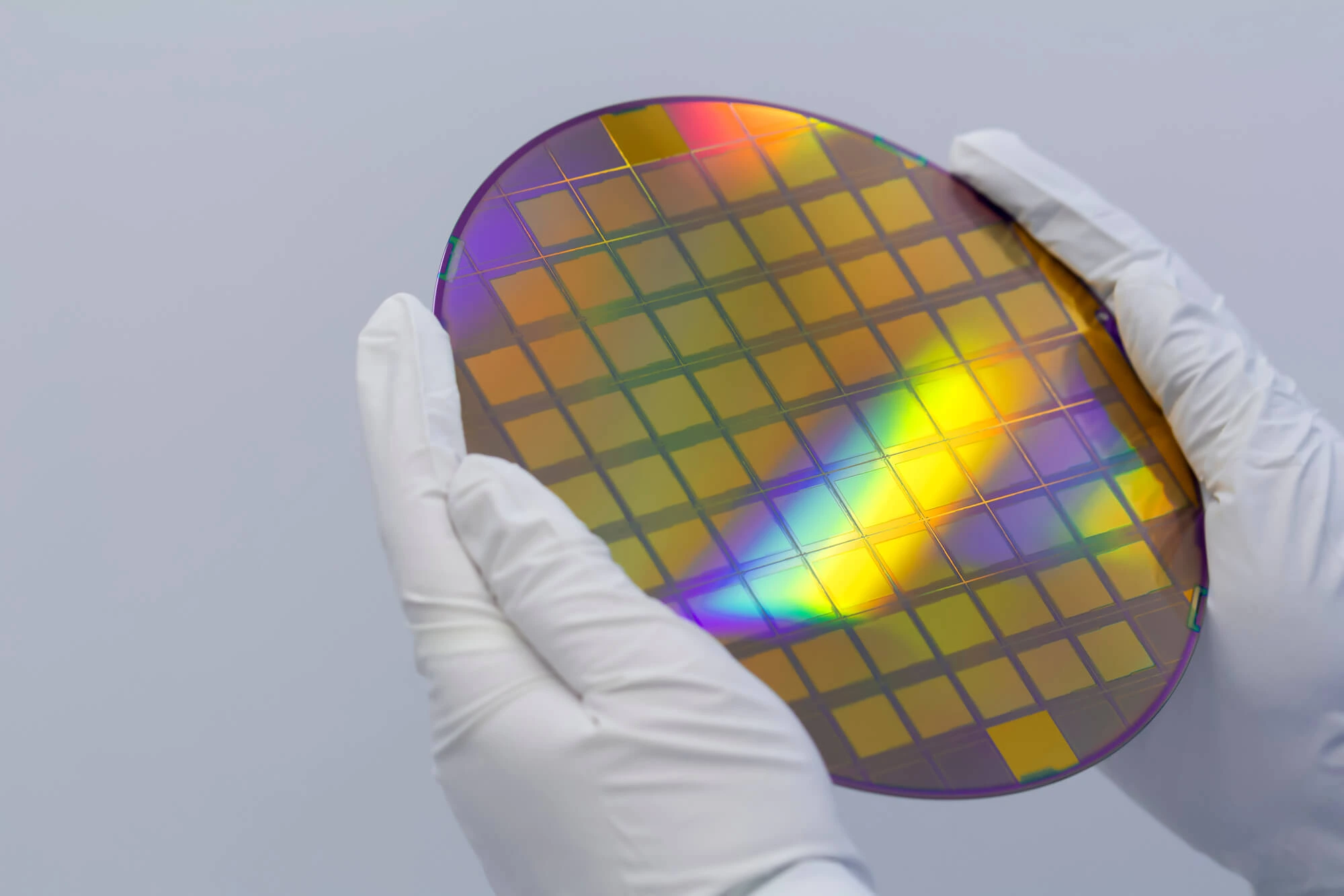
Understanding the challenges and ideal packing methods when transporting GaAs reclaim wafers is key to preventing damage.
Read More