.jpg)
Stay up-to-date with the latest news and trends in wafer and semiconductor technologies.
*Blogs are for educational and informational purposes ONLY
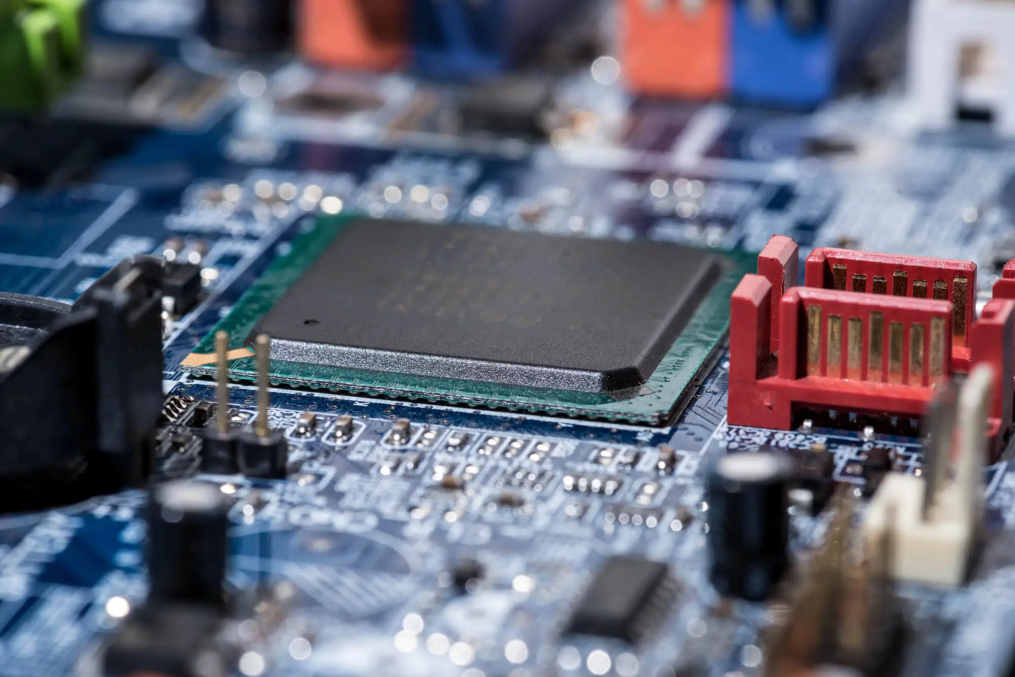
Bonding substrates from silicon wafer suppliers can produce more effective, durable, and comprehensive chips. Here are some bonding techniques worth knowing about.
Read More
Behind the spurt of more realistic AI generators lies the growth in wafer manufacturing. Here, we’ll explain the role of wafers in AI images.
Read More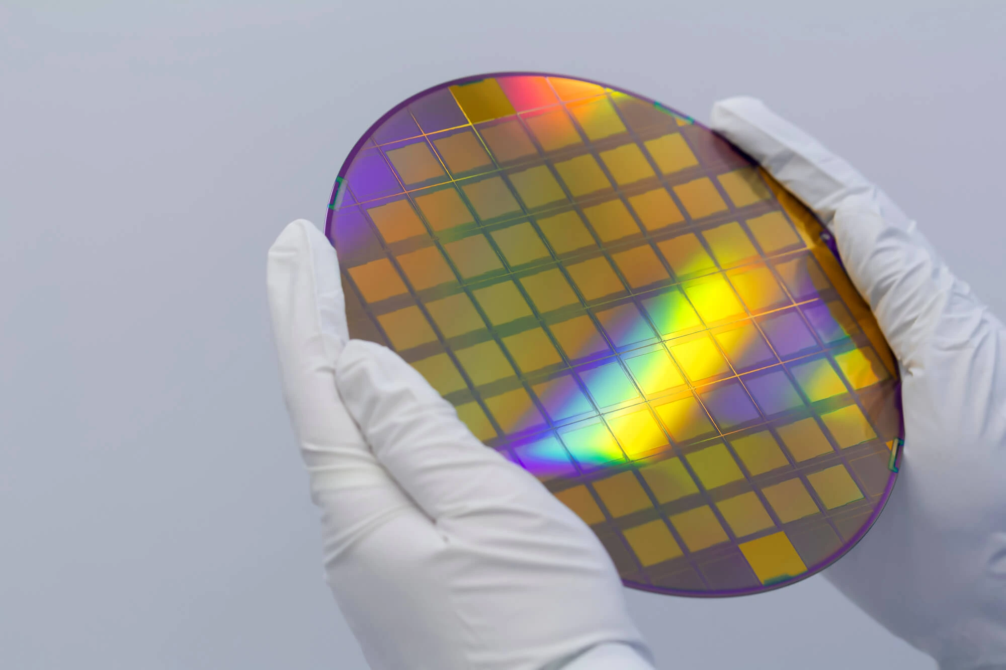
Understanding the challenges and ideal packing methods when transporting GaAs reclaim wafers is key to preventing damage.
Read More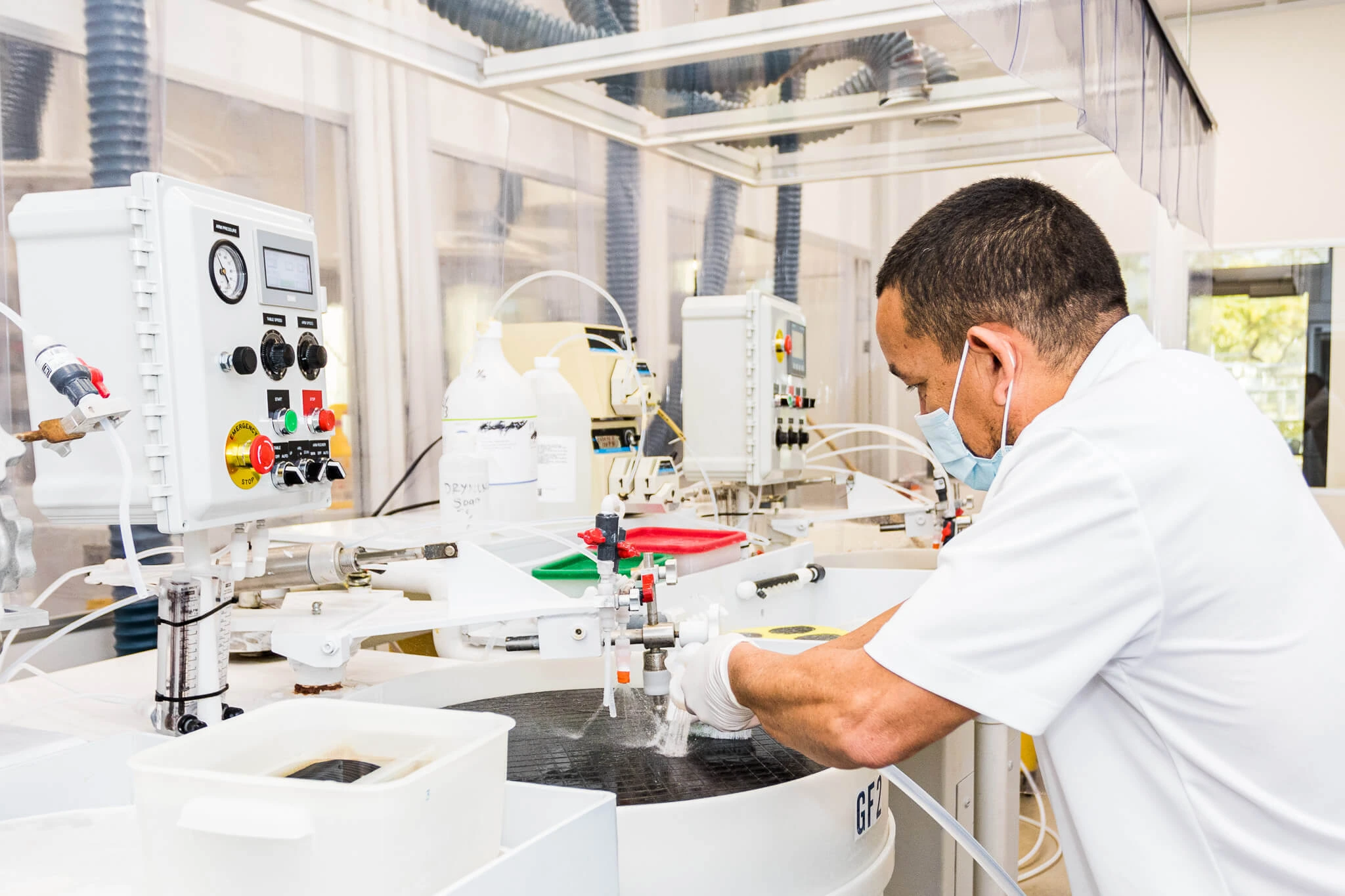
Different materials have different thermal cycles, from CZ silicon and GaAs to a float zone wafer. Understanding that is key when manufacturing semiconductors.
Read More
When manufacturing complex substrates with a silicon wafer, the wafer-to-wafer bonding technique is crucial—but what does this method involve?
Read More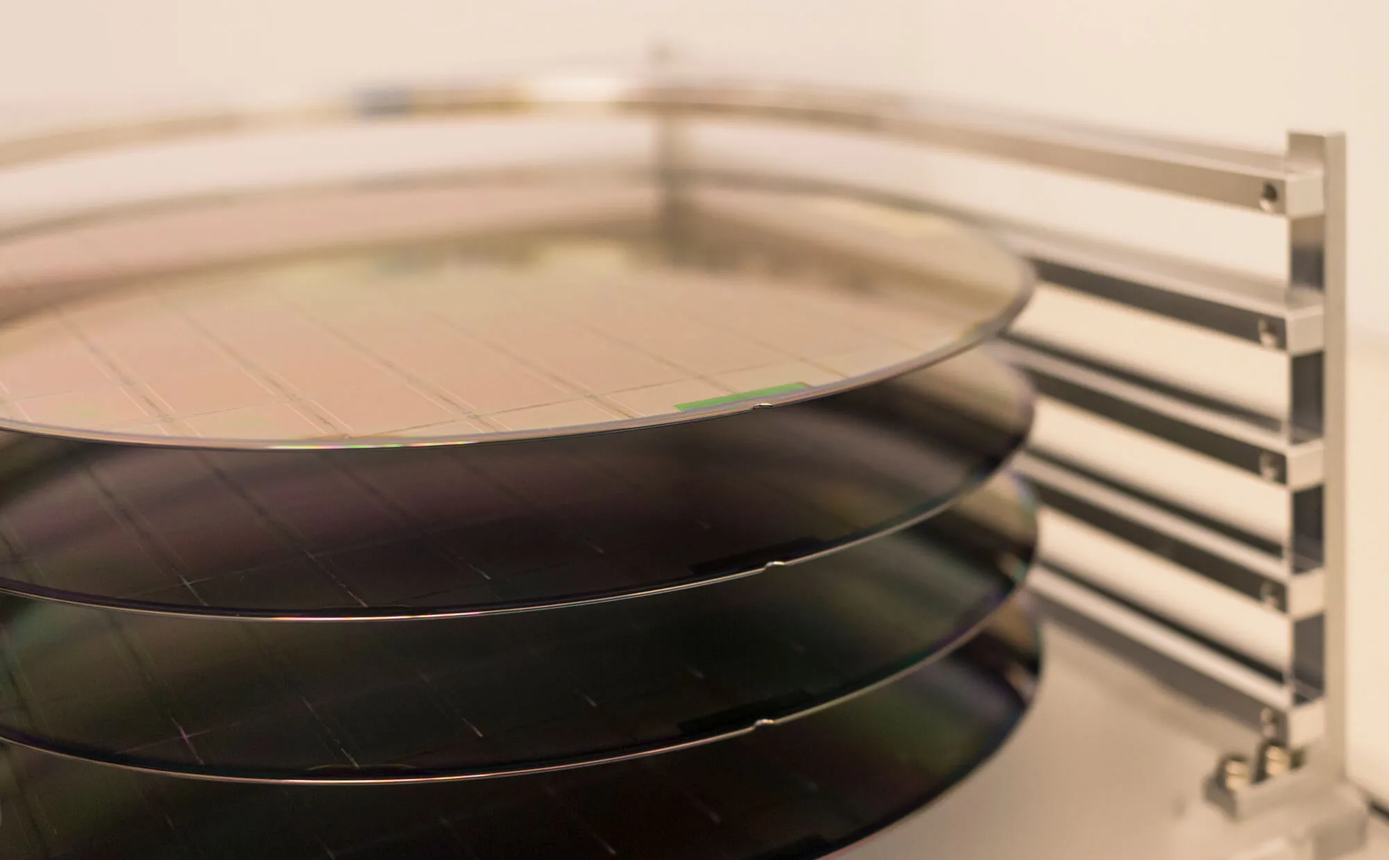
Before manufacturing InP reclaim wafers, fabs analyze each substrate in detail to ensure its high quality. Here are some signs we look out for.
Read More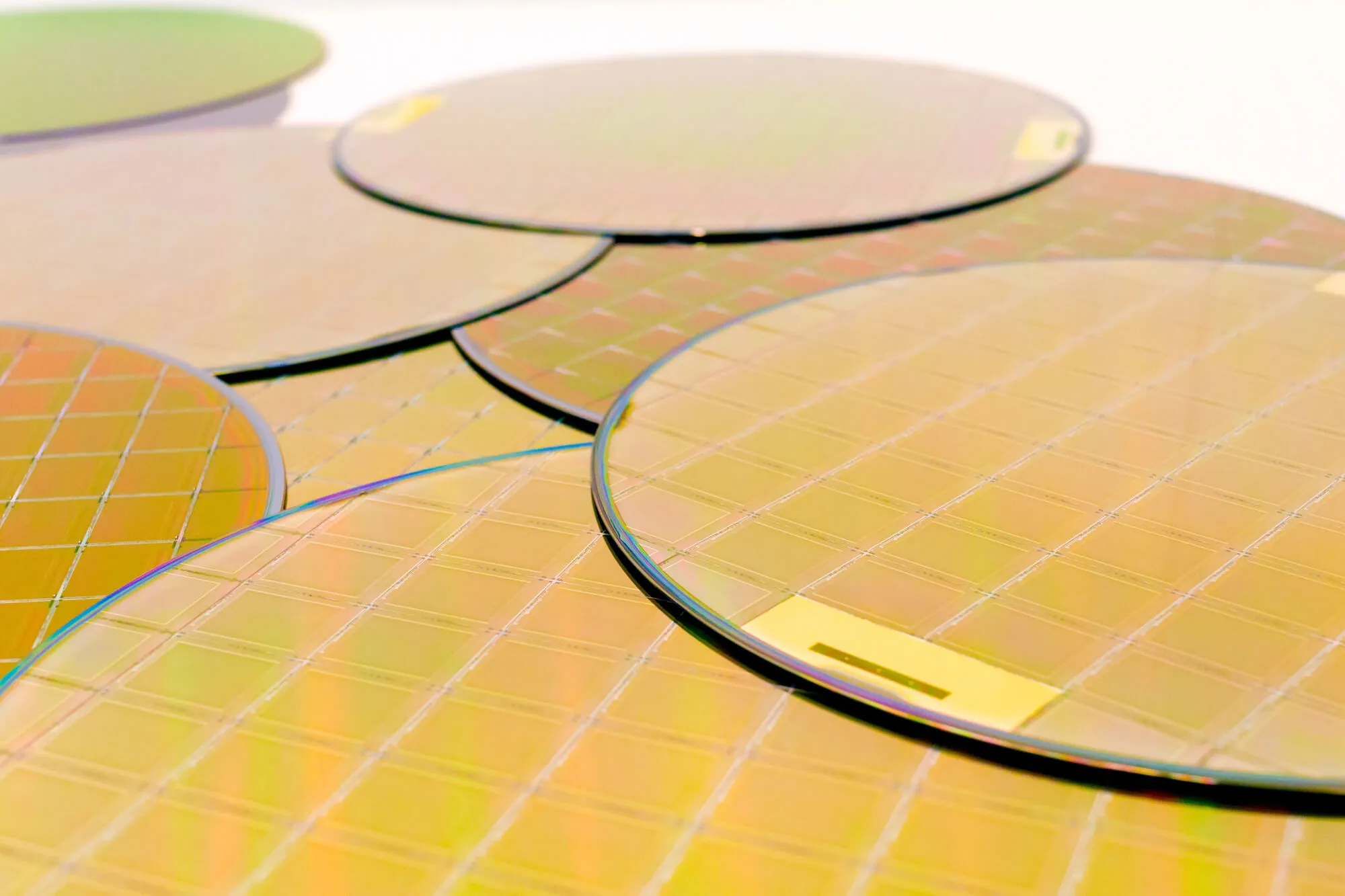
The process for making thin silicon wafers often starts with CZ silicon growth, which produces high-purity silicon with a monocrystalline structure.
Read More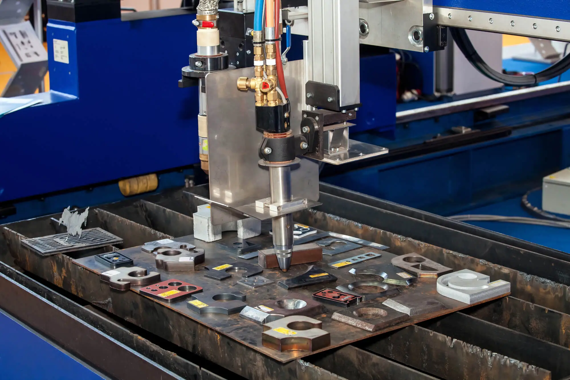
Ablation is a wafer laser marking technique used to remove material from the substrate and leave a readable mark. Here, we’ll explain when this method is preferred.
Read More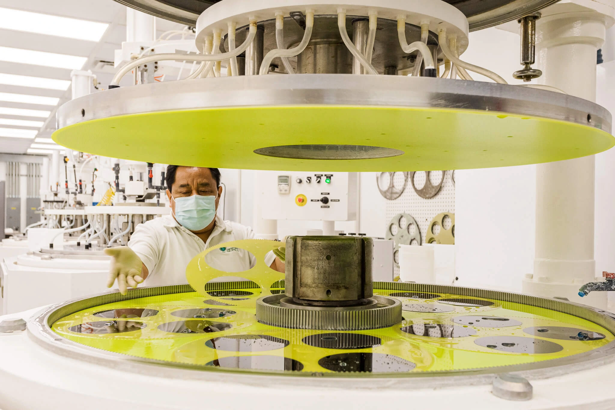
InP wafers are widely used in high-speed electronics, optical communication, and photonic devices, but they are more complex to process than silicon, and here are five reasons why.
Read More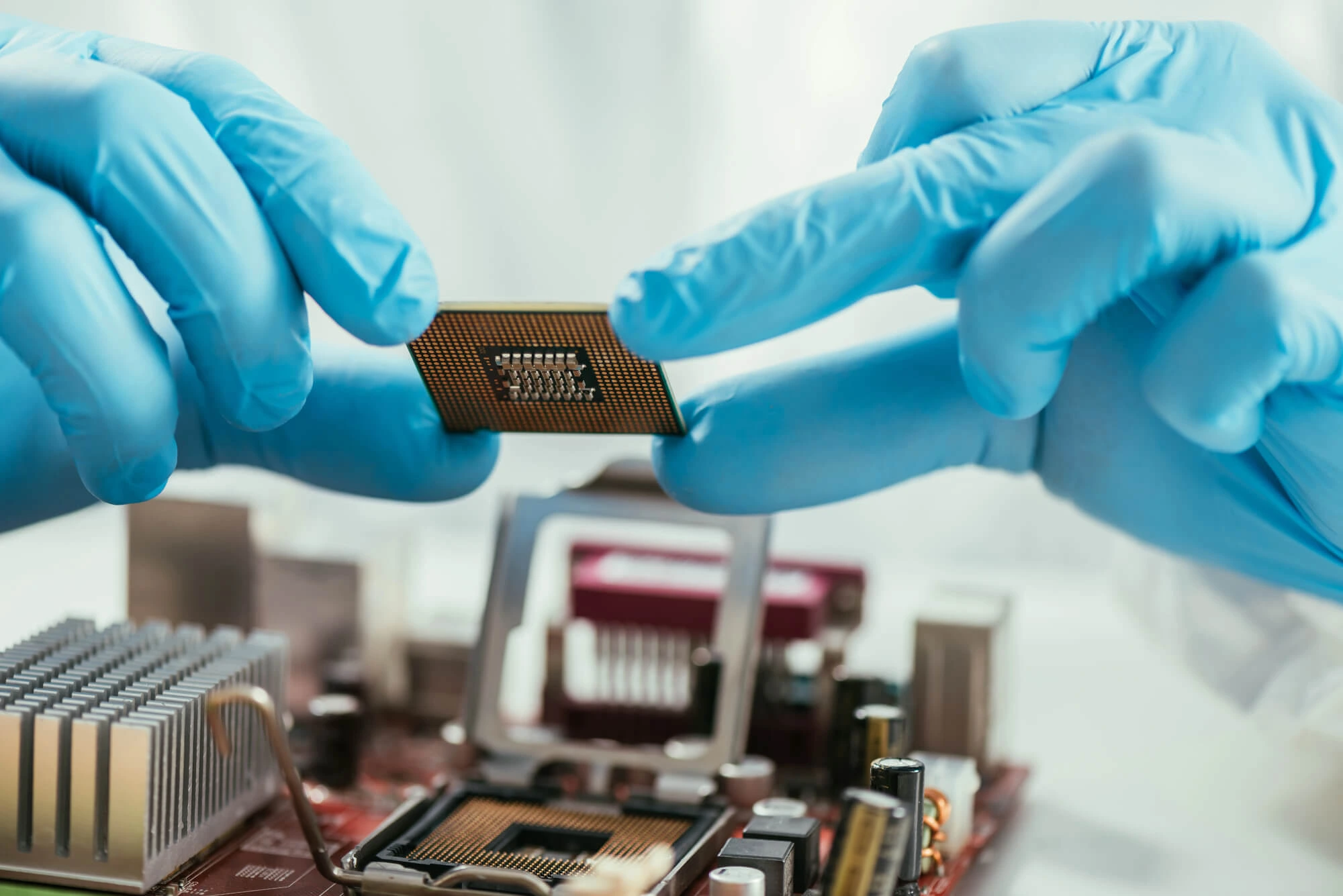
Double side polishing ensures precision and consistency in semiconductors. But, for what chips and transistors rely on a double side polish wafer to function?
Read More


